Block diagram, Hardware, I/o port internal peripheral functions – Renesas 4514 User Manual
Page 19: 4500 series cpu core
1-6
HARDWARE
4513/4514 Group User’s Manual
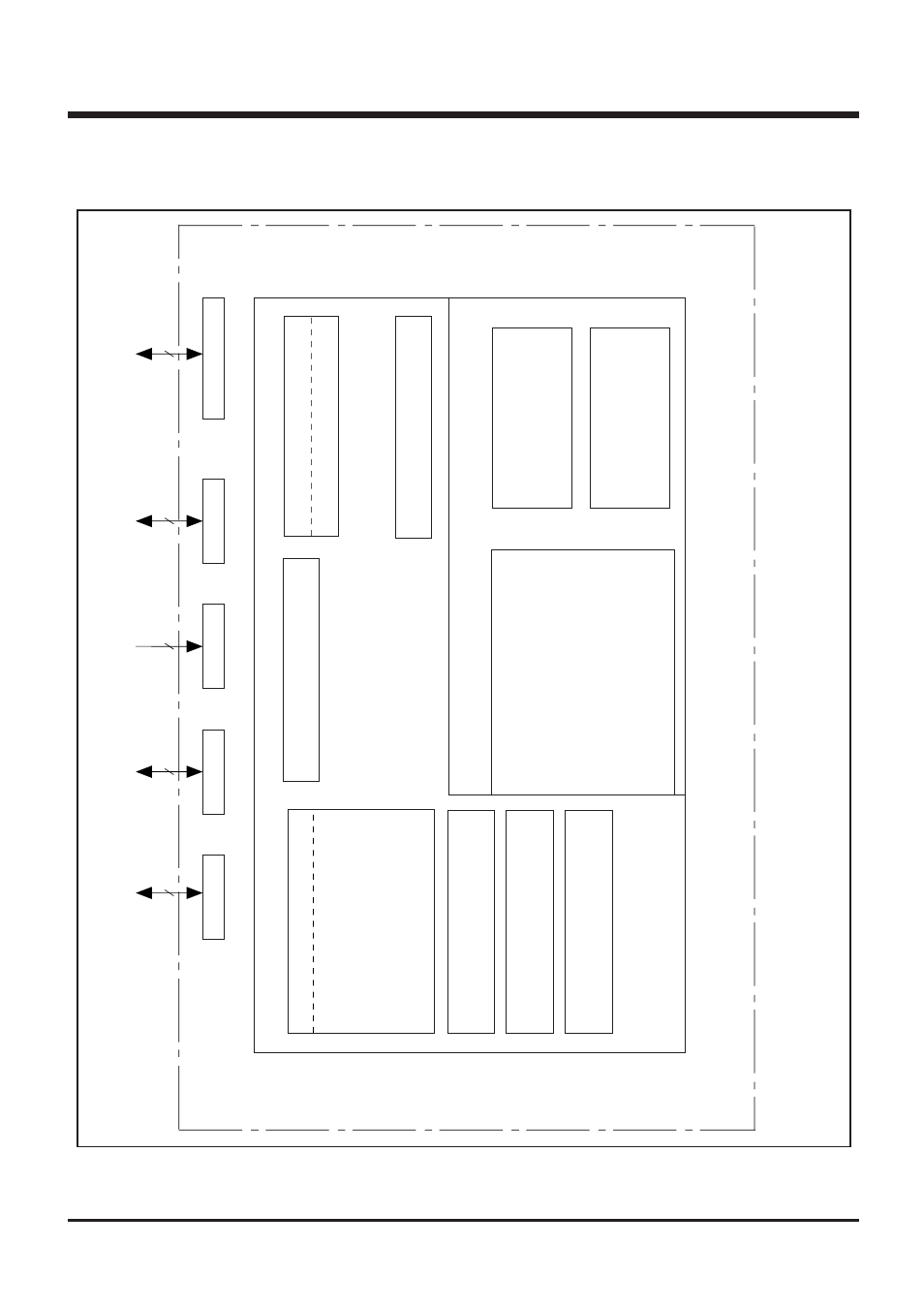
BLOCK DIAGRAM (4513 Group)
|[go
1
Voltage drop detection circuit
4
S
e
ri
a
l I/O
(8
b
its
✕
1)
Voltage comparator
(2 circuits)
X
IN
–X
OUT
I/O port
Internal peripheral functions
Timer
System clock generating circuit
Watchdog timer
(16 bits)
Memory
ROM
2048, 4096,6144, 8192
words
×
10 bits
RAM
128, 256, 384 words
×
4 bits
4500 Series
CPU core
ALU (4 bits)
Register A (4 bits) Register B (4 bits)
Register D (3 bits) Register E (8 bits)
Stack register SK (8 levels)
Interrupt stack register SDP (1 level)
Timer 1 (8 bits)
Timer 2 (8 bits)
Timer 3 (8 bits)
Timer 4 (8 bits)
A-D converter
(10 bits
✕
4 ch)
Port D
Port P3
Port P2
Port P1
Port P0
4
3
2
8
BLOCK DIAGRAM
This manual is related to the following products: