Serial i/o, Hardware, Function block operations – Renesas 4514 User Manual
Page 49
1-36
HARDWARE
4513/4514 Group User’s Manual
FUNCTION BLOCK OPERATIONS
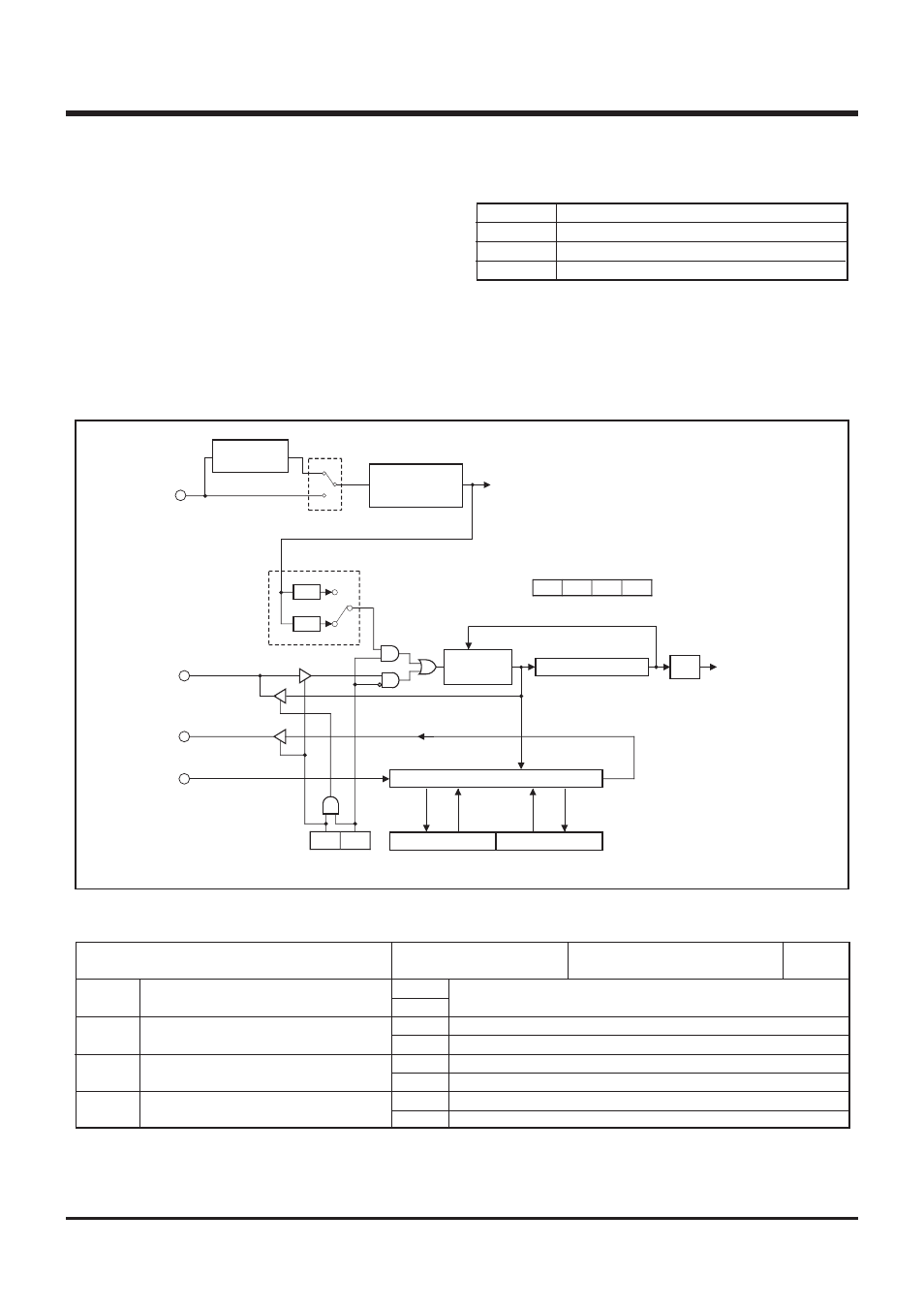
SERIAL I/O
The 4513/4514 Group has a built-in clock synchronous serial I/O
which can serially transmit or receive 8-bit data.
Serial I/O consists of;
• serial I/O register SI
• serial I/O mode register J1
• serial I/O transmission/reception completion flag (SIOF)
• serial I/O counter
Registers A and B are used to perform data transfer with internal
CPU, and the serial I/O pins are used for external data transfer.
The pin functions of the serial I/O pins can be set with the register
J1.
Table 11 Serial I/O pins
Pin
P2
0
/S
CK
P2
1
/S
OUT
P2
2
/S
IN
Pin function when selecting serial I/O
Clock I/O (S
CK
)
Serial data output (S
OUT
)
Serial data input (S
IN
)
Note: Input ports P2
0
–P2
2
can be used regardless of register J1.
Fig. 22 Serial I/O structure
Table 12 Serial I/O mode register
J1
3
J1
2
J1
1
J1
0
Serial I/O mode register J1
This bit has no function, but read/write is enabled.
Instruction clock signal divided by 8
Instruction clock signal divided by 4
Input ports P2
0
, P2
1
, P2
2
selected
Serial I/O ports S
CK
, S
OUT
, S
IN
/input ports P2
0
, P2
1
, P2
2
selected
External clock
Internal clock (instruction clock divided by 4 or 8)
Not used
Serial I/O internal clock dividing ratio
selection bit
Serial I/O port selection bit
Serial I/O synchronous clock selection bit
at reset : 0000
2
at RAM back-up : state retained
Note: “R” represents read enabled, and “W” represents write enabled.
0
1
0
1
0
1
0
1
R/W
J1
2
SIOF
J1
2
J1
1
J1
0
J1
1
J1
0
MSB
1/4
1/8
1
0
P2
1
/S
OUT
P2
2
/S
IN
P2
0
/S
CK
TSIAB
TABSI
S
OUT
S
IN
S
CK
J1
3
MR
3
1
0
X
IN
Division circuit
(divided by 2)
Internal clock
generation circuit
(divided by 3)
Instruction clock
Serial I/O mode register J1
Serial I/O interrupt
Serial I/O counter (3)
Synchronous
circuit
Register B (4)
Register A (4)
Serial I/O register SI (8)
LSB
Note: The output structure of S
CK
and S
OUT
pins is N-channel open-drain.