Rom ordering method, Hardware, Function block operations/rom ordering method – Renesas 4514 User Manual
Page 71

1-58
HARDWARE
4513/4514 Group User’s Manual
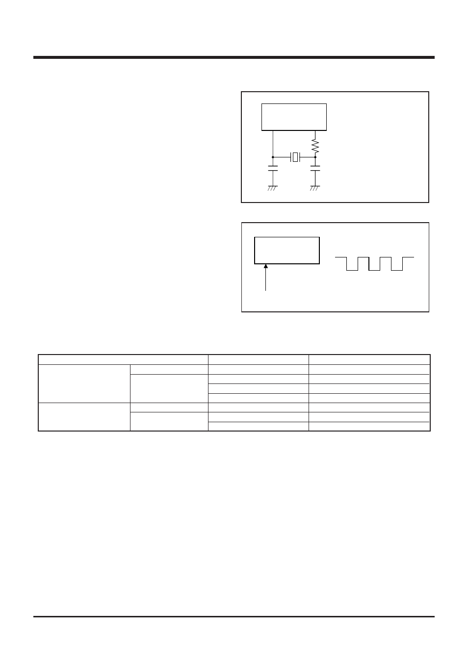
Clock signal f(X
IN
) is obtained by externally connecting a ceramic
resonator.
Connect this external circuit to pins X
IN
and X
OUT
at the shortest
distance. A feedback resistor is built in between pins X
IN
and X
OUT
.
When an external clock signal is input, connect the clock source to
X
IN
and leave X
OUT
open. When using an external clock, the maxi-
mum value of external clock oscillating frequency is shown in Table
24.
Table 24 Maximum value of external clock oscillation frequency
Supply voltage
V
DD
= 2.0 V to 5.5 V
V
DD
= 4.0 V to 5.5 V
V
DD
= 2.5 V to 5.5 V
V
DD
= 2.0 V to 5.5 V
V
DD
= 2.5 V to 5.5 V
V
DD
= 4.0 V to 5.5 V
V
DD
= 2.5 V to 5.5 V
Oscillation frequency (duty ratio)
3.0 MHz (40 % to 60 %)
3.0 MHz (40 % to 60 %)
1.0 MHz (40 % to 60 %)
0.8 MHz (40 % to 60 %)
3.0 MHz (40 % to 60 %)
3.0 MHz (40 % to 60 %)
1.0 MHz (40 % to 60 %)
ROM ORDERING METHOD
Please submit the information described below when ordering
Mask ROM.
(1) Mask ROM Order Confirmation Form ..................................... 1
(2) Data to be written into mask ROM ............................... EPROM
(three sets containing the identical data)
(3) Mark Specification Form .......................................................... 1
Fig. 42 Ceramic resonator external circuit
Fig. 43 External clock input circuit
N o t e : E x t e r n a l l y c o n n e c t a
damping resistor Rd de-
pending on the oscillation
frequency.
(A feedback resistor is
built-in.)
Use the resonator manu-
facturer’s recommended
value because constants
such as capacitance de-
pend on the resonator.
Mask ROM version
One Time PROM version
4513/4514
X
IN
X
OUT
Rd
C
IN
C
OUT
4513/4514
X
IN
X
OUT
External oscillation circuit
V
DD
V
SS
Middle-speed mode
High-speed mode
Middle-speed mode
High-speed mode
FUNCTION BLOCK OPERATIONS/ROM ORDERING METHOD
