Symbol, Hardware – Renesas 4514 User Manual
Page 75
1-62
HARDWARE
4513/4514 Group User’s Manual
SYMBOL
The symbols shown below are used in the following instruction function table and instruction list.
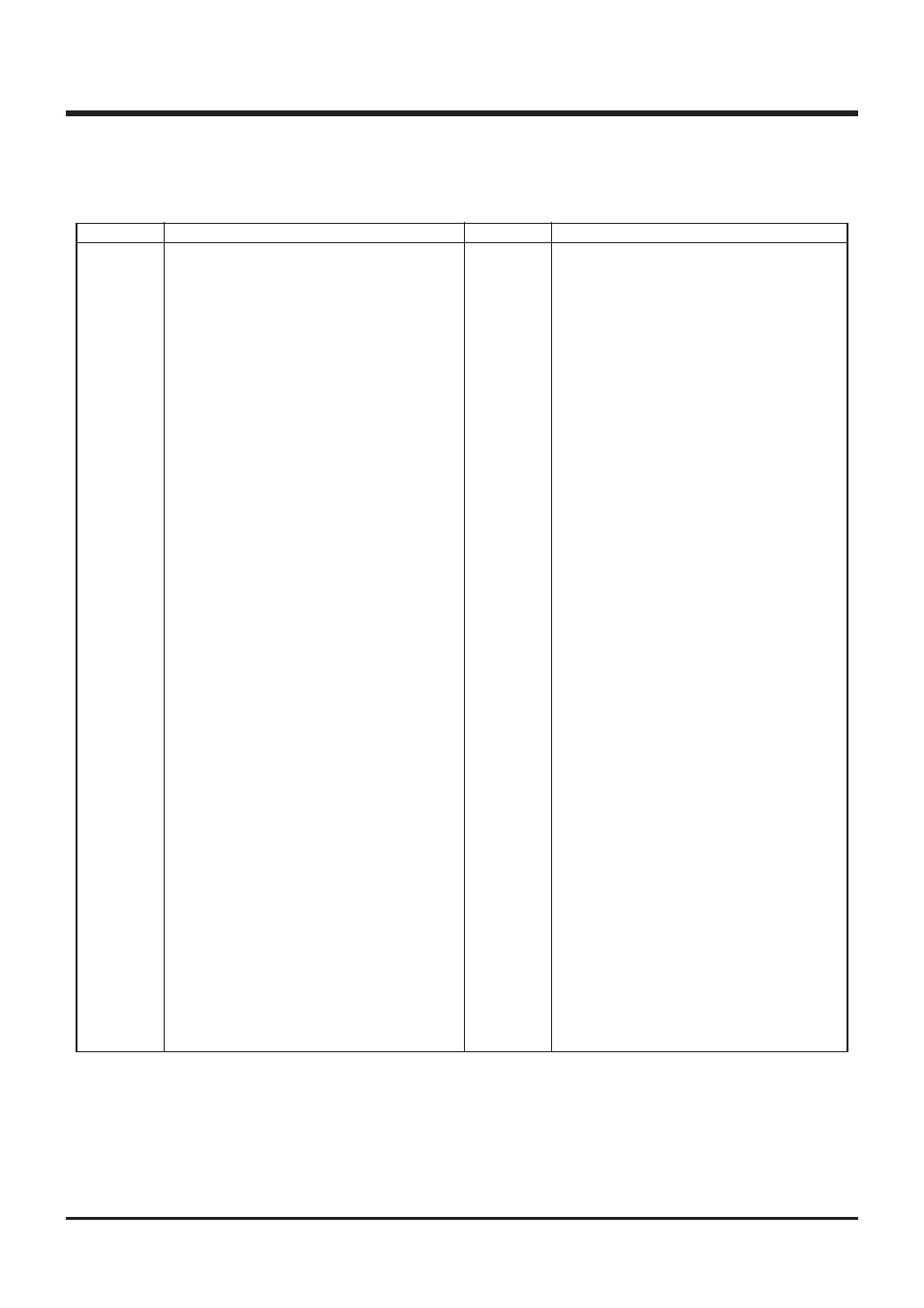
Symbol
A
B
DR
E
Q1
Q2
Q3
AD
J1
SI
V1
V2
I1
I2
W1
W2
W3
W4
W6
MR
K0
PU0
FR0
X
Y
Z
DP
PC
PC
H
PC
L
SK
SP
CY
R1
R2
R3
R4
T1
T2
T3
T4
Contents
Register A (4 bits)
Register B (4 bits)
Register D (3 bits)
Register E (8 bits)
A-D control register Q1 (4 bits)
A-D control register Q2 (4 bits)
Voltage comparator control register Q3 (4 bits)
Successive comparison register AD (10 bits)
Serial I/O mode register J1 (4 bits)
Serial I/O register SI (8 bits)
Interrupt control register V1 (4 bits)
Interrupt control register V2 (4 bits)
Interrupt control register I1 (4 bits)
Interrupt control register I2 (4 bits)
Timer control register W1 (4 bits)
Timer control register W2 (4 bits)
Timer control register W3 (4 bits)
Timer control register W4 (4 bits)
Timer control register W6 (4 bits)
Clock control register MR (4 bits)
Key-on wakeup control register K0 (4 bits)
Pull-up control register PU0 (4 bits)
Direction register FR0 (4 bits)
Register X (4 bits)
Register Y (4 bits)
Register Z (2 bits)
Data pointer (10 bits)
(It consists of registers X, Y, and Z)
Program counter (14 bits)
High-order 7 bits of program counter
Low-order 7 bits of program counter
Stack register (14 bits
✕
8)
Stack pointer (3 bits)
Carry flag
Timer 1 reload register
Timer 2 reload register
Timer 3 reload register
Timer 4 reload register
Timer 1
Timer 2
Timer 3
Timer 4
Contents
Timer 1 interrupt request flag
Timer 2 interrupt request flag
Timer 3 interrupt request flag
Timer 4 interrupt request flag
Watchdog timer flag
Watchdog timer enable flag
Interrupt enable flag
External 0 interrupt request flag
External 1 interrupt request flag
Power down flag
A-D conversion completion flag
Serial I/O transmission/reception completion flag
Port D (8 bits)
Port P0 (4 bits)
Port P1 (4 bits)
Port P2 (3 bits)
Port P3 (4 bits)
Port P4 (4 bits)
Port P5 (4 bits)
Hexadecimal variable
Hexadecimal variable
Hexadecimal variable
Hexadecimal variable
Hexadecimal constant
Hexadecimal constant
Hexadecimal constant
Binary notation of hexadecimal variable A
(same for others)
Direction of data movement
Data exchange between a register and memory
Decision of state shown before “?”
Contents of registers and memories
Negate, Flag unchanged after executing instruction
RAM address pointed by the data pointer
Label indicating address a
6
a
5
a
4
a
3
a
2
a
1
a
0
Label indicating address a
6
a
5
a
4
a
3
a
2
a
1
a
0
in page p
5
p
4
p
3
p
2
p
1
p
0
Hex. C + Hex. number x (also same for others)
Symbol
T1F
T2F
T3F
T4F
WDF1
WEF
INTE
EXF0
EXF1
P
ADF
SIOF
D
P0
P1
P2
P3
P4
P5
x
y
z
p
n
i
j
A
3
A
2
A
1
A
0
←
↔
?
( )
—
M(DP)
a
p, a
C
+
x
Note : The 4513/4514 Group just invalidates the next instruction when a skip is performed. The contents of program counter is not increased by 2. Accord-
ingly, the number of cycles does not change even if skip is not performed. However, the cycle count becomes “1” if the TABP p, RT, or RTS instruction
is skipped.
SYMBOL