Multifunction, Connections of unused pins, Hardware – Renesas 4514 User Manual
Page 23: Pin description
1-10
HARDWARE
4513/4514 Group User’s Manual
Notes 1: Pins except above have just single function.
2: The input of D
6
, D
7
, P2
0
–P2
2
, CMP0-, CMP0+, CMP1-, CMP1+ and the input/output of P3
0
, P3
1
, P4
0
–P4
3
can be used even when CNTR0, CNTR1,
S
CK
, S
OUT
, S
IN
, INT0, INT1, and A
IN0
–A
IN7
are selected.
3: The 4513 Group does not have P4
0
/A
IN4
–P4
3
/A
IN7
.
Notes 1: After system is released from reset, port P5 is in an input mode (di-
rection register FR0 = 0000
2
)
2: When the P0
0
–P0
3
and P1
0
–P1
3
are connected to V
SS
, turn off
their pull-up transistors (register PU0i=“0”) and also invalidate the
key-on wakeup functions (register K0i=“0”) by software. When
these pins are connected to V
SS
while the key-on wakeup func-
tions are left valid, the system fails to return from RAM back-up
state. When these pins are open, turn on their pull-up transistors
(register PU0i=“1”) by software, or set the output latch to “0.”
Be sure to select the key-on wakeup functions and the pull-up
functions with every two pins. If only one of the two pins for the
key-on wakeup function is used, turn on their pull-up transistors by
software and also disconnect the other pin. (i = 0, 1, 2, or 3.)
(Note when the output latch is set to “0” and pins are open)
●
After system is released from reset, port is in a high-impedance state un-
til it is set the output latch to “0” by software. Accordingly, the voltage
level of pins is undefined and the excess of the supply current may occur
while the port is in a high-impedance state.
●
To set the output latch periodically by software is recommended because
value of output latch may change by noise or a program run away
(caused by noise).
(Note when connecting to V
SS
and V
DD
)
●
Connect the unused pins to V
SS
and V
DD
using the thickest wire at the
shortest distance against noise.
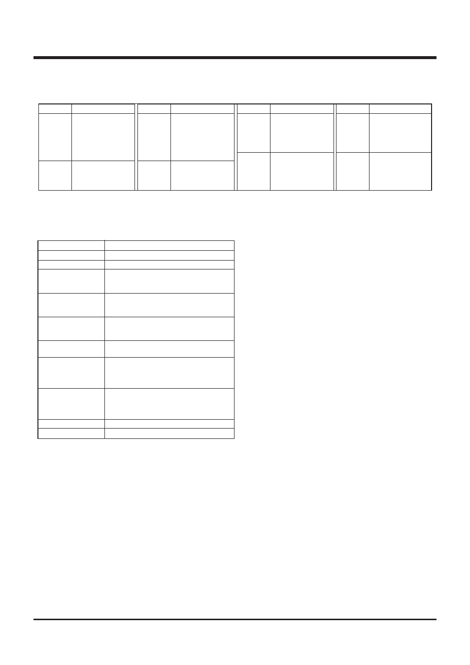
Pin
D
6
D
7
P2
0
P2
1
P2
2
P3
0
P3
1
Multifunction
CNTR0
CNTR1
S
CK
S
OUT
S
IN
INT0
INT1
MULTIFUNCTION
Multifunction
CMP0-
CMP0+
CMP1-
CMP1+
A
IN4
A
IN5
A
IN6
A
IN7
Pin
A
IN0
A
IN1
A
IN2
A
IN3
P4
0
P4
1
P4
2
P4
3
CONNECTIONS OF UNUSED PINS
Connection
Open (when using an external clock).
Connect to V
SS
.
Connect to V
SS
, or set the output latch to
“0” and open.
Connect to V
SS
.
Connect to V
SS
, or set the output latch to
“0” and open.
Connect to V
SS
, or set the output latch to
“0” and open.
When the input mode is selected by soft-
ware, pull-up to V
DD
through a resistor or
pull-down to V
DD
.
When selecting the output mode, open.
Connect to V
SS
.
Open or connect to V
SS
(Note 2)
Open or connect to V
SS
(Note 2)
Pin
X
OUT
VDCE
D
0
–D
5
D
6
/CNTR0
D
7
/CNTR1
P2
0
/S
CK
P2
1
/S
OUT
P2
2
/S
IN
P3
0
/INT0
P3
1
/INT1
P3
2
, P3
3
P4
0
/A
IN4
–P4
3
/A
IN7
P5
0
–P5
3
(Note 1)
A
IN0
/CMP0-
A
IN1
/CMP0+
A
IN2
/CMP1-
A
IN3
/CMP1+
P0
0
–P0
3
P1
0
–P1
3
Pin
CNTR0
CNTR1
S
CK
S
OUT
S
IN
INT0
INT1
Multifunction
D
6
D
7
P2
0
P2
1
P2
2
P3
0
P3
1
Multifunction
A
IN0
A
IN1
A
IN2
A
IN3
P4
0
P4
1
P4
2
P4
3
Pin
CMP0-
CMP0+
CMP1-
CMP1+
A
IN4
A
IN5
A
IN6
A
IN7
PIN DESCRIPTION