Appendix, Noise – Renesas 4514 User Manual
Page 192

4513/4514 Group User’s Manual
APPENDIX
3-25
3.4 Notes on noise
(3)
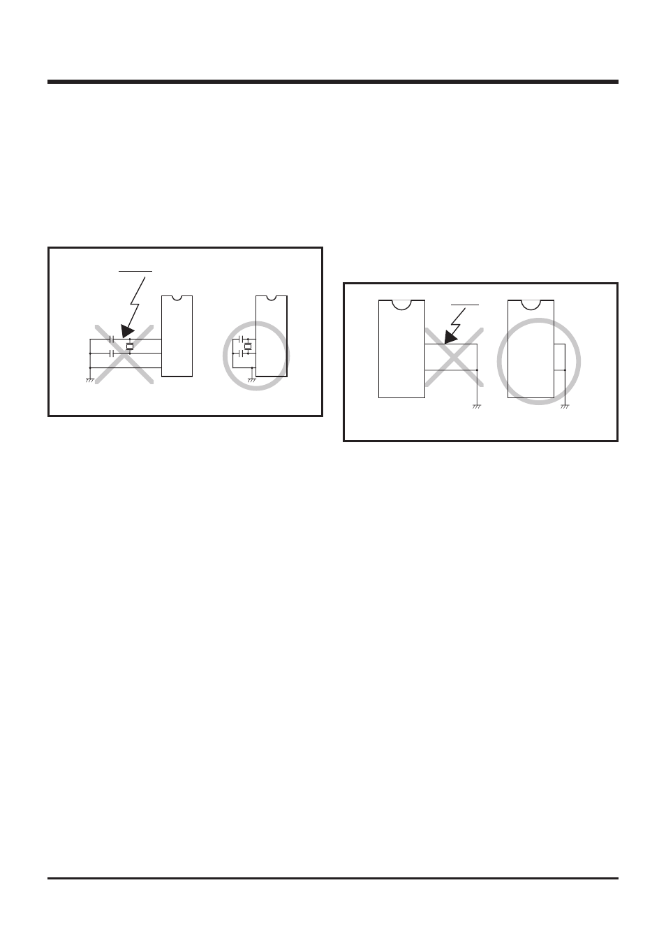
Wiring for clock input/output pins
• Make the length of wiring which is connected
to clock I/O pins as short as possible.
• Make the length of wiring across the
grounding lead of a capacitor which is
connected to an oscillator and the V
SS
pin
of a microcomputer as short as possible.
• Separate the V
SS
pattern only for oscillation
from other V
SS
patterns.
Fig. 3.4.3 Wiring for clock I/O pins
●
Reason
If noise enters clock I/O pins, clock
waveforms may be deformed. This may
cause a program failure or program runaway.
Also, if a potential difference is caused by
the noise between the V
SS
level of a
microcomputer and the V
SS
level of an
oscillator, the correct clock will not be input
in the microcomputer.
Fig. 3.4.4 Wiring for CNV
SS
pin
Noise
X
IN
X
OUT
V
SS
X
IN
X
OUT
V
SS
N.G.
O.K.
Noise
CNV
SS
V
SS
CNV
SS
V
SS
N.G.
O.K.
(4)
Wiring to CNV
SS
pin
Connect the CNV
SS
pin to the V
SS
pin with
the shortest possible wiring.
●
Reason
The operation mode of a microcomputer is
influenced by a potential at the CNV
SS
pin.
If a potential difference is caused by the
noise between pins CNV
SS
and V
SS
, the
operation mode may become unstable. This
may cause a microcomputer malfunction or
a program runaway.
