Hardware, Function block operations, 1) power-on reset – Renesas 4514 User Manual
Page 63: 2) internal state at reset, Internal reset signal, Watchdog timer output v, Or less

1-50
HARDWARE
4513/4514 Group User’s Manual
FUNCTION BLOCK OPERATIONS
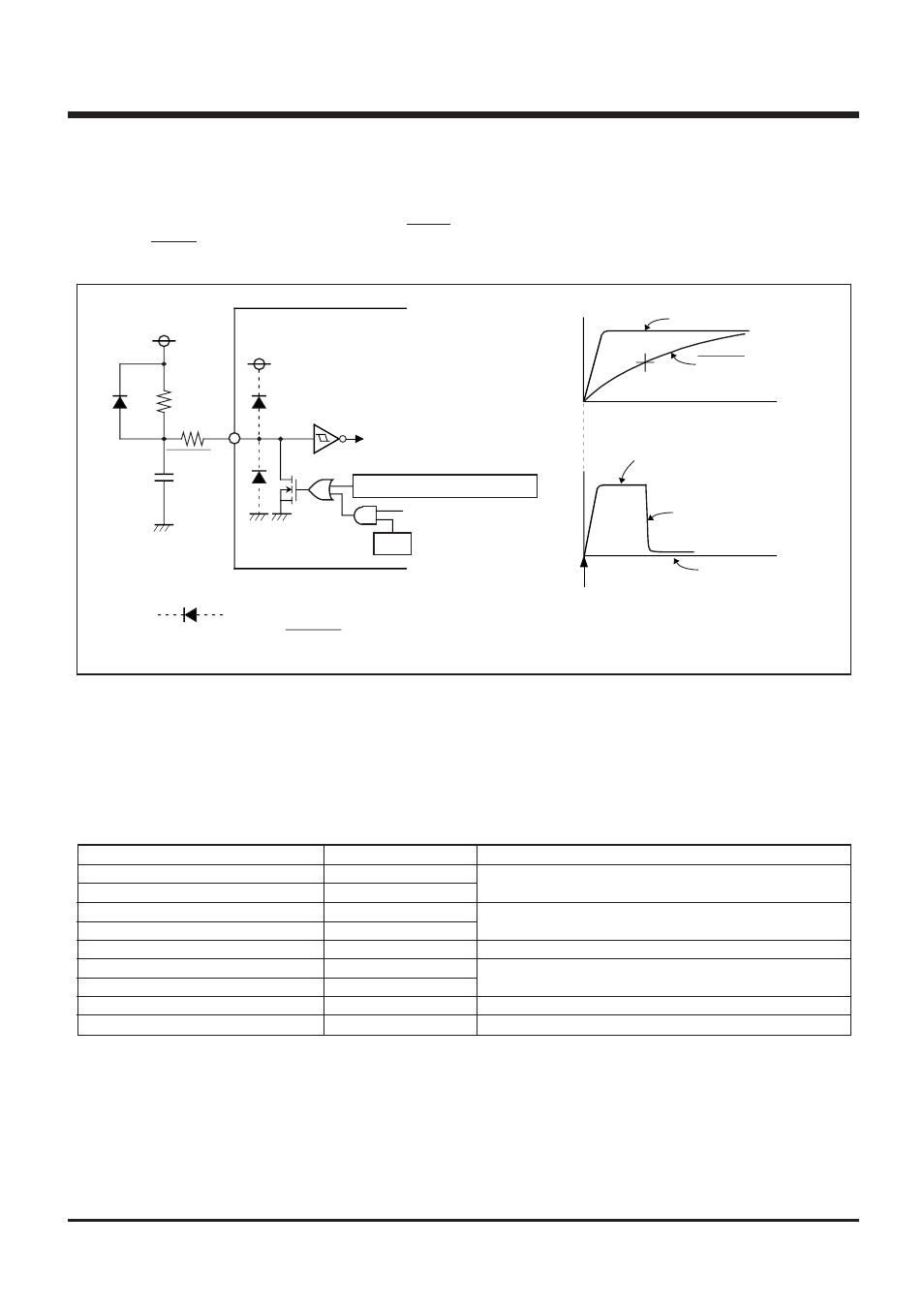
(1) Power-on reset
Reset can be performed automatically at power on (power-on re-
set) by connecting resistors, a diode, and a capacitor to RESET
pin. Connect RESET pin and the external circuit at the shortest dis-
tance.
Fig. 34 Power-on reset circuit example
(2) Internal state at reset
Table 19 shows port state at reset, and Figure 35 shows inter nal
state at reset (they are the same after system is released from re-
set). The contents of timers, registers, flags and RAM except
shown in Figure 35 are undefined, so set the initial value to them.
Table 19 Port state at reset
Name
D
0
–D
5
D
6
/CNTR0, D
7
/CNTR1
P0
0
–P0
3
P1
0
–P1
3
P2
0
/S
CK
, P2
1
/S
OUT
, P2
2
/S
IN
P3
0
/INT0, P3
1
/INT1
P3
2
, P3
3
(Note 4)
P4
0
/A
IN4
–P4
3
/A
IN7
(Note 4)
P5
0
–P5
3
(Note 4)
Notes 1: Output latch is set to “1.”
2: Pull-up transistor is turned OFF.
3: After system is released from reset, port P5 is in the input mode. (Direction register FR0 = 0000
2
)
4: The 4513 Group does not have these ports.
Function
D
0
–D
5
D
6
, D
7
P0
0
–P0
3
P1
0
–P1
3
P2
0
–P2
2
P3
0
, P3
1
P3
2
, P3
3
P4
0–
P4
3
P5
0
–P5
3
State
High impedance (Note)
High impedance (Notes 1, 2)
High impedance
High impedance (Note 1)
High impedance (Note 1)
High impedance (Note 3)
V
D D
RESET pin
WEF
(Note)
Internal reset signal
Voltage drop detection circuit
Watchdog timer output
V
DD
RESET pin voltage
Power-on
Reset released
Internal reset signal
Reset state
Note:
This symbol represents a parasitic diode.
Applied potential to RESET pin must be V
DD
or less.
