10 oscillation circuit, 1 oscillation circuit, Application – Renesas 4514 User Manual
Page 166
APPLICATION
2-63
4513/4514 Group User’s Manual
2.10 Oscillation circuit
2.10 Oscillation circuit
The 4513/4514 Group has an internal oscillation circuit to produce the clock required for microcomputer
operation.
The clock signal f(X
IN
) is obtained by connecting a ceramic resonator to X
IN
pin and X
OUT
pin.
2.10.1 Oscillation circuit
(1)
f(X
IN
) clock generating circuit
The clock signal f(X
IN
) is obtained by connecting a ceramic resonator externally.
Connect this external circuit to pins X
IN
and X
OUT
at the shortest distance. A feed-back resistor is
built-in between X
IN
pin and X
OUT
pin.
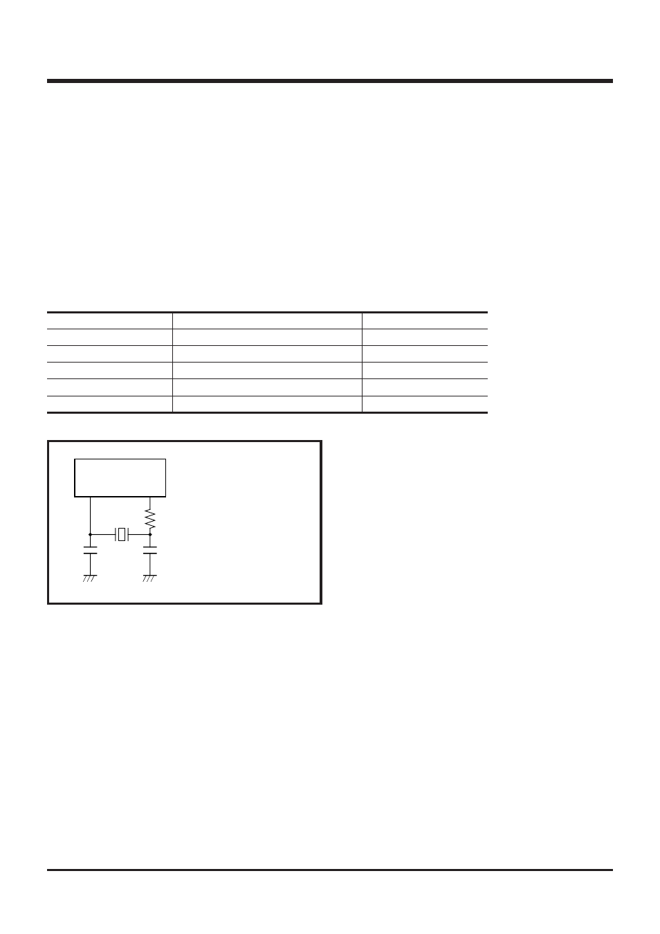
Figure 2.10.1 shows an example of an oscillation circuit connecting a ceramic resonator externally.
Keep the maximum value of oscillation frequency within the range listed Table 2.10.1.
Supply voltage
2.5 V to 5.5 V
4.0 V to 5.5 V
2.5 V to 5.5 V
2.0 V to 5.5 V (Note)
2.0 V to 5.5 V (Note)
(System clock)
(f(X
IN
)/2) Middle-speed mode
(f(X
IN
))
High-speed mode
(f(X
IN
))
High-speed mode
(f(X
IN
)/2) Middle-speed mode
(f(X
IN
))
High-speed mode
Oscillation frequency
4.2 MHz
4.2 MHz
2.0 MHz
3.0 MHz
1.5 MHz
Note: 2.5 V to 5.5 V for the One Timer PROM version.
Table 2.10.1 Maximum value of oscillation frequency and supply voltage
Fig. 2.10.1 Oscillation circuit example connecting
ceramic resonator externally
Note: Externally connect a
damping resistor Rd de-
pending on the oscilla-
tion frequency. (A feed-
back resistor is built-in.)
U s e t h e r e s o n a t o r
manufacturer’s recom-
mended value because
constants such as ca-
pacitance depend on the
resonator.
4513/4514
X
IN
X
OUT
Rd
C
IN
C
OUT