Hardware, Control registers – Renesas 4514 User Manual
Page 100
4513/4514 Group User’s Manual
HARDWARE
1-87
K0
3
K0
2
K0
1
K0
0
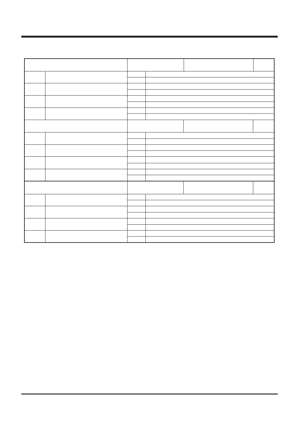
Key-on wakeup control register K0
PU0
3
PU0
2
PU0
1
PU0
0
Key-on wakeup not used
Key-on wakeup used
Key-on wakeup not used
Key-on wakeup used
Key-on wakeup not used
Key-on wakeup used
Key-on wakeup not used
Key-on wakeup used
Pins P1
2
and P1
3
key-on wakeup
control bit
Pins P1
0
and P1
1
key-on wakeup
control bit
Pins P0
2
and P0
3
key-on wakeup
control bit
Pins P0
0
and P0
1
key-on wakeup
control bit
at reset : 0000
2
at RAM back-up : state retained
0
1
0
1
0
1
0
1
Pull-up transistor OFF
Pull-up transistor ON
Pull-up transistor OFF
Pull-up transistor ON
Pull-up transistor OFF
Pull-up transistor ON
Pull-up transistor OFF
Pull-up transistor ON
Pins P1
2
and P1
3
pull-up transistor
control bit
Pins P1
0
and P1
1
pull-up transistor
control bit
Pins P0
2
and P0
3
pull-up transistor
control bit
Pins P0
0
and P0
1
pull-up transistor
control bit
R/W
Pull-up control register PU0
at reset : 0000
2
at RAM back-up : state retained
0
1
0
1
0
1
0
1
R/W
Notes 1: “R” represents read enabled, and “W” represents write enabled.
2: The 4513 Group does not have the direction register FR0.
FR0
3
FR0
2
FR0
1
FR0
0
Port P5
3
input
Port P5
3
output
Port P5
2
input
Port P5
2
output
Port P5
1
input
Port P5
1
output
Port P5
0
input
Port P5
0
output
Port P5
3
input/output control bit
Port P5
2
input/output control bit
Port P5
1
input/output control bit
Port P5
0
input/output control bit
Direction register FR0 (Note 2)
at reset : 0000
2
at RAM back-up : state retained
0
1
0
1
0
1
0
1
W
CONTROL REGISTERS