Pin description, Hardware – Renesas 4514 User Manual
Page 22
4513/4514 Group User’s Manual
HARDWARE
1-9
PIN DESCRIPTION
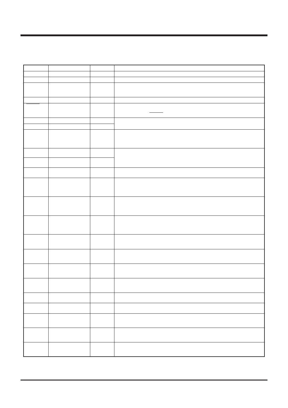
Name
Power supply
Ground
Voltage drop detec-
tion circuit enable
CNV
SS
Reset input
System clock input
System clock output
I/O port D
(Input is examined
by skip decision.)
I/O port P0
I/O port P1
Input port P2
I/O port P3
I/O port P4
I/O port P5
Analog input
Timer input/output
Timer input/output
Interrupt input
Serial data input
Serial data output
Serial I/O clock
input/output
Voltage comparator
input
Voltage comparator
input
Pin
V
DD
V
SS
VDCE
CNV
SS
RESET
X
IN
X
OUT
D
0
–D
7
P0
0
–P0
3
P1
0
–P1
3
P2
0
–P2
2
P3
0
–P3
3
P4
0
–P4
3
P5
0
–P5
3
A
IN0
–A
IN7
CNTR0
CNTR1
INT0, INT1
S
IN
S
OUT
S
CK
CMP0-
CMP0+
CMP1-
CMP1+
Input/Output
—
—
Input
—
I/O
Input
Output
I/O
I/O
I/O
Input
I/O
I/O
I/O
Input
I/O
I/O
Input
Input
Output
I/O
Input
Input
Function
Connected to a plus power supply.
Connected to a 0 V power supply.
VDCE pin is used to control the operation/stop of the voltage drop detection circuit.
When “H” level is input to this pin, the circuit is operating. When “L” level is inpu to
this pin, the circuit is stopped.
Connect CNV
SS
to V
SS
and apply “L” (0V) to CNV
SS
certainly.
An N-channel open-drain I/O pin for a system reset. When the watchdog timer
causes the system to be reset or system reset is performed by the voltage drop de-
tection circuit, the RESET pin outputs “L” level.
I/O pins of the system clock generating circuit. X
IN
and X
OUT
can be connected to
ceramic resonator. A feedback resistor is built-in between them.
Each pin of port D has an independent 1-bit wide I/O function. Each pin has an out-
put latch. For input use, set the latch of the specified bit to “1.” The output structure
is N-channel open-drain.
Ports D
6
and D
7
are also used as CNTR0 and CNTR1, respectively.
Each of ports P0 and P1 serves as a 4-bit I/O port, and it can be used as inputs
when the output latch is set to “1.” The output structure is N-channel open-drain.
Every pin of the ports has a key-on wakeup function and a pull-up function. Both
functions can be switched by software.
3-bit input port. Ports P2
0
, P2
1
and P2
2
are also used as S
CK
, S
OUT
and S
IN
, re-
spectively.
4-bit I/O port (2-bit I/O port for the 4513 Group). For input use, set the latch of the
specified bit to “1.” The output structure is N-channel open-drain. Ports P3
0
and
P3
1
are also used as INT0 and INT1, respectively.
The 4513 Group does not have ports P3
2
, P3
3
.
4-bit I/O port. For input use, set the latch of the specified bit to “1.” The output
structure is N-channel open-drain. Ports P4
0
–P4
3
are also used as analog input
pins A
IN4
–A
IN7
, respectively.
The 4513 Group does not have port P4.
4-bit I/O port. Each pin has a direction register and an independent 1-bit wide I/O
function. For input use, set the direction register to “0.” For output use, set the di-
rection regiser to “1.” The output structure is CMOS.
The 4513 Group does not have port P5.
Analog input pins for A-D converter. A
IN0
–A
IN3
are also used as voltage compara-
tor input pins and A
IN4
–A
IN7
are also used as port P4.
The 4513 Group does not have A
IN4
–A
IN7
.
CNTR0 pin has the function to input the clock for the timer 2 event counter, and to
output the timer 1 underflow signal divided by 2.
CNTR0 pin is also used as port D
6
.
CNTR1 pin has the function to input the clock for the timer 4 event counter, and to
output the timer 3 underflow signal divided by 2.
CNTR1 pin is also used as port D
7
.
INT0, INT1 pins accept external interrupts. They also accept the input signal to re-
turn the system from the RAM back-up state.
INT0, INT1 pins are also used as ports P3
0
and P3
1
, respectively.
S
IN
pin is used to input serial data signals by software.
S
IN
pin is also used as port P2
2
.
S
OUT
pin is used to output serial data signals by software.
S
OUT
pin is also used as port P2
1
.
S
CK
pin is used to input and output synchronous clock signals for serial data trans-
fer by software.
S
CK
pin is also used as port P2
0
.
CMP0-, CMP0+ pins are used as the voltage comparator input pin when the volt-
age comparator function is selected by software.
CMP0-, CMP0+ pins are also used as A
IN0
and A
IN1
.
CMP1-, CMP1+ pins are used as the voltage comparator input pin when the volt-
age comparator function is selected by software.
CMP1-, CMP1+ pins are also used as A
IN2
and A
IN3
.
PIN DESCRIPTION