1 related registers, Application, 5 a-d converter – Renesas 4514 User Manual
Page 153
APPLICATION
2.5 A-D converter
2-50
4513/4514 Group User’s Manual
2.5.1 Related registers
(1)
A-D control register Q1
Analog input pin selection bits are assigned to register Q1.
Set the contents of this register through register A with the TQ1A instruction. The TAQ1 instruction
can be used to transfer the contents of register Q1 to register A.
Table 2.5.1 shows the A-D control register Q1.
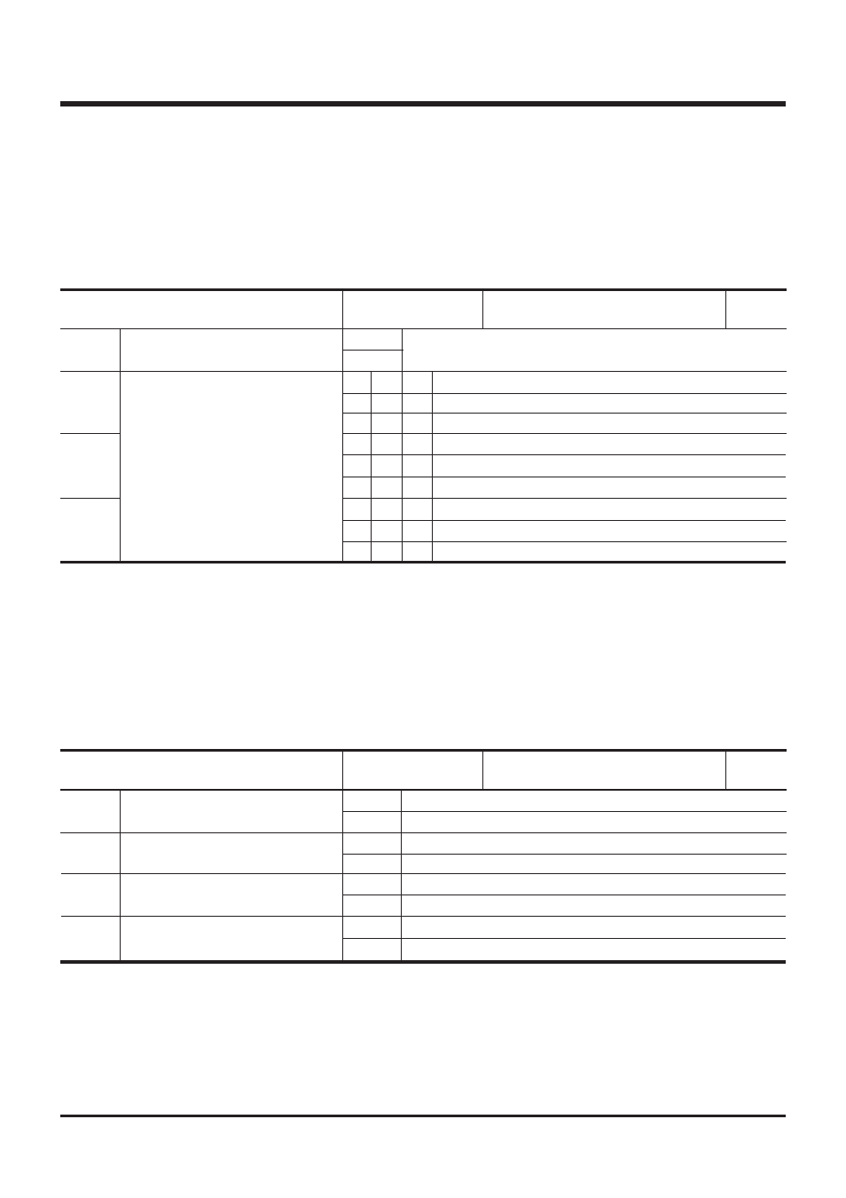
Table 2.5.1 A-D control register Q1
A-D control register Q1
at reset : 0000
2
at power down : state retained
R/W
Not used
Analog input pin selection bits
(Note 2)
Q1
3
Q1
2
Q1
1
Q1
0
0
1
Notes 1: “R” represents read enabled, and “W” represents write enabled.
2: Select A
IN4
–A
IN7
with register Q1 after setting register Q2.
(2)
A-D control register Q2
Analog input pin selection bits and A-D operation mode control bit are assigned to register Q2.
Set the contents of this register through register A with the TQ2A instruction. The TAQ2 instruction
can be used to transfer the contents of register Q2 to register A.
Table 2.5.2 shows the A-D control register Q2.
Table 2.5.2 A-D control register Q2
Q1
2
0
0
0
0
1
1
1
1
Q1
1
0
0
1
1
0
0
1
1
This bit has no function, but read/write is enabled.
Selected pin
A
IN0
A
IN1
A
IN2
A
IN3
A
IN4
(Not available for 4513 Group)
A
IN5
(Not available for 4513 Group)
A
IN6
(Not available for 4513 Group)
A
IN7
(Not available for 4513 Group)
Q1
0
0
1
0
1
0
1
0
1
A-D control register Q2
at reset : 0000
2
at power down : state retained
R/W
A-D operation mode control bit
P4
3
/A
IN7
, P4
2
/A
IN6
pin function
selection bit (Note 3)
P4
1
/A
IN5
pin function selection bit
(Note 3)
P4
0
/A
IN4
pin function selection bit
(Note 3)
Q2
3
Q2
2
Q2
1
Q2
0
0
1
0
1
0
1
0
1
Notes 1: “R” represents read enabled, and “W” represents write enabled.
2: Select A
IN4
–A
IN7
with register Q1 after setting register Q2.
3: In the 4513 Group, these bits are not used.
4: In the 4513 Group, only read/write of these bits is enabled.
A-D conversion mode
Comparator mode
P4
3
, P4
2
(I/O) (Note 4)
A
IN7
, A
IN6
/P4
3
, P4
2
(Output) (Note 4)
P4
1
(I/O) (Note 4)
A
IN5
/P4
1
(Output) (Note 4)
P4
0
(I/O) (Note 4)
A
IN4
/P4
0
(Output) (Note 4)