Port function, Definition of clock and cycle, Hardware – Renesas 4514 User Manual
Page 24: Pin description
4513/4514 Group User’s Manual
HARDWARE
1-11
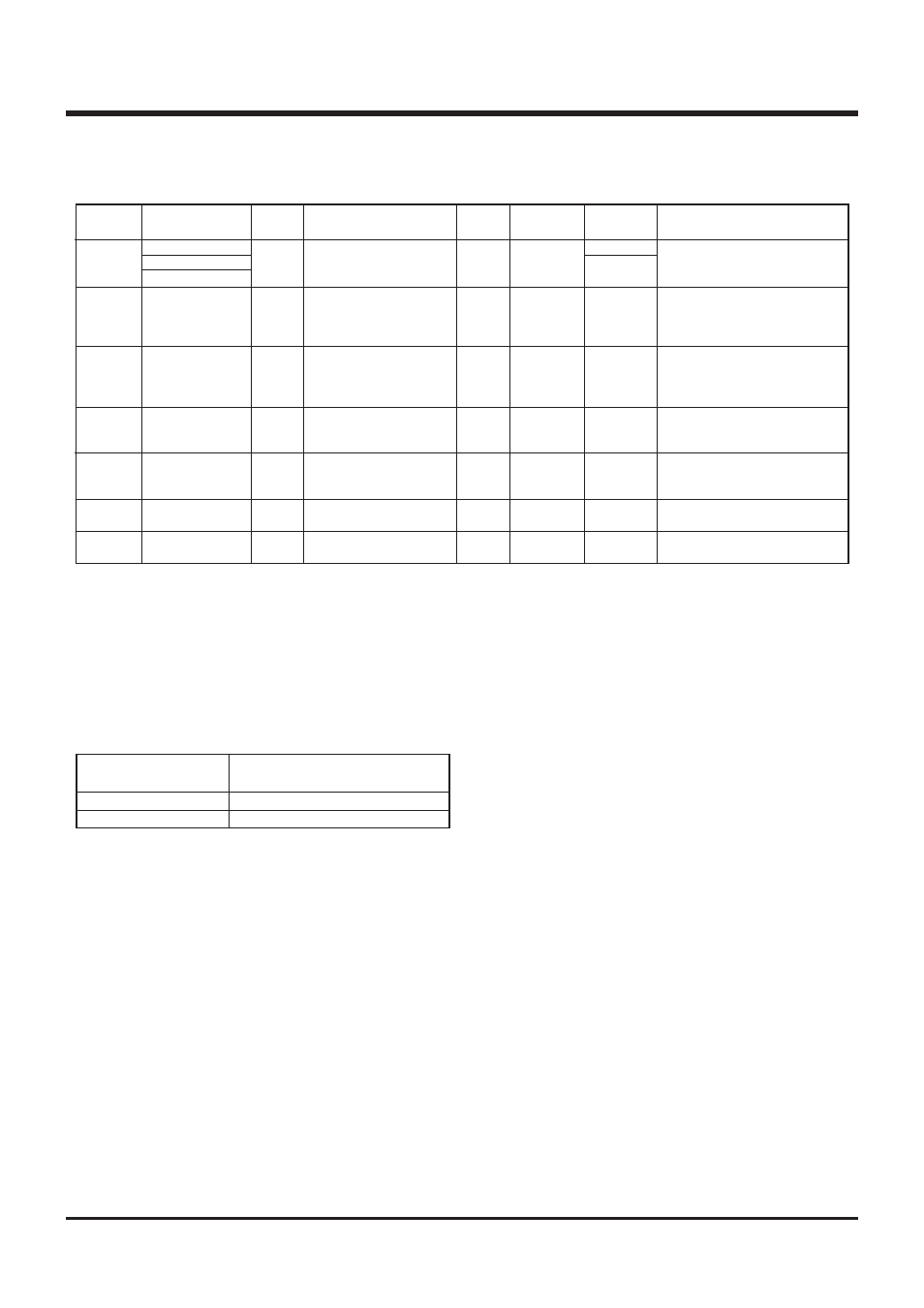
Notes 1: The 4513 Group does not have P3
2
and P3
3
.
2: The 4513 Group does not have these ports.
DEFINITION OF CLOCK AND CYCLE
●
System clock
The system clock is the basic clock for controlling this product.
The system clock is selected by the bit 3 of the clock control reg-
ister MR.
PORT FUNCTION
Port
Port D
Port P0
Port P1
Port P2
Port P3
(Note 1)
Port P4
(Note 2)
Port P5
(Note 2)
I/O
unit
1
4
4
3
4
4
4
Control
instructions
SD, RD
SZD
CLD
OP0A
IAP0
OP1A
IAP1
IAP2
OP3A
IAP3
OP4A
IAP4
OP5A
IAP5
Control
registers
W6
PU0, K0
PU0, K0
J1
I1, I2
Q2
FR0
Output structure
N-channel open-drain
N-channel open-drain
N-channel open-drain
N-channel open-drain
N-channel open-drain
CMOS
Input
Output
I/O
(8)
I/O
(4)
I/O
(4)
Input
(3)
I/O
(4)
I/O
(4)
I/O
(4)
Remark
Built-in programmable pull-up
functions
Key-on wakeup functions
(programmable)
Built-in programmable pull-up
functions
Key-on wakeup functions
(programmable)
Built-in key-on wakeup
function
(P3
0
/INT0, P3
1
/INT1)
Pin
D
0
–D
5
D
6
/CNTR0
D
7
/CNTR1
P0
0
–P0
3
P1
0
–P1
3
P2
0
/S
CK
P2
1
/S
OUT
P2
2
/S
IN
P3
0
/INT0
P3
1
/INT1
P3
2
, P3
3
P4
0
/A
IN4
–P4
3
/A
IN7
P5
0
–P5
3
Register MR
MR
3
0
1
System clock
f(X
IN
)
f(X
IN
)/2
Note: f(X
IN
)/2 is selected after system is released from reset.
●
Instruction clock
The instruction clock is a signal derived by dividing the system
clock by 3. The one instruction clock cycle generates the one
machine cycle.
●
Machine cycle
The machine cycle is the standard cycle required to execute the
instruction.
Table Selection of system clock
PIN DESCRIPTION