Hardware, Control registers – Renesas 4514 User Manual
Page 98

4513/4514 Group User’s Manual
HARDWARE
1-85
0
1
0
1
0
1
0
1
W2
1
0
0
1
1
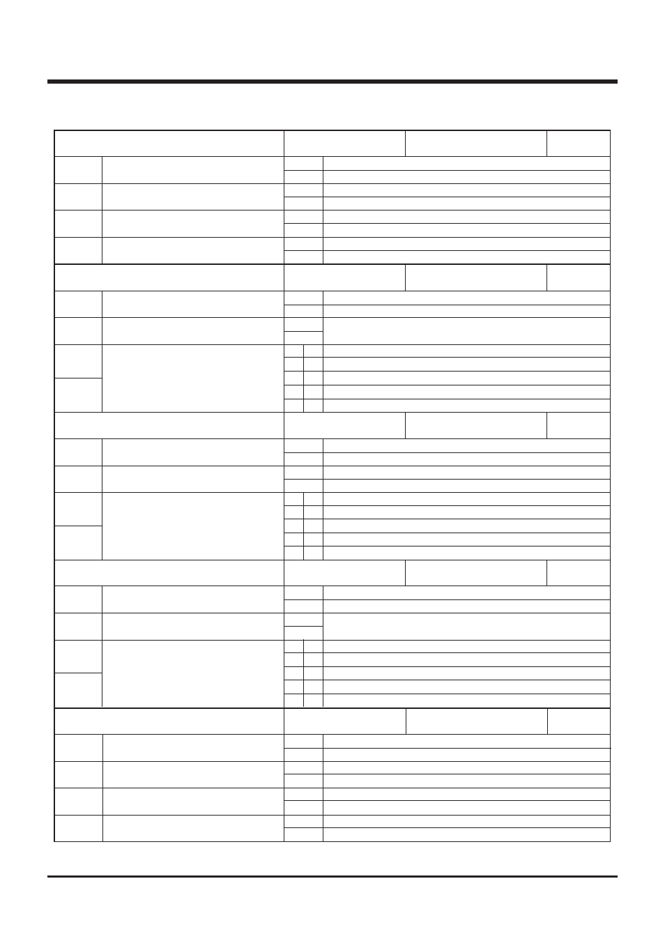
Stop (state initialized)
Operating
Instruction clock divided by 4
Instruction clock divided by 16
Stop (state retained)
Operating
Count start synchronous circuit not selected
Count start synchronous circuit selected
Prescaler control bit
Prescaler dividing ratio selection bit
Timer 1 control bit
Timer 1 count start synchronous circuit
control bit
Stop (state retained)
Operating
This bit has no function, but read/write is enabled.
Count source
Timer 1 underflow signal
Prescaler output
CNTR0 input
16 bit timer (WDT) underflow signal
Timer 2 control bit
Not used
Timer 2 count source selection bits
0
1
0
1
W2
0
0
1
0
1
W1
3
W1
2
W1
1
W1
0
W2
3
W2
2
W2
1
W2
0
W3
3
W3
2
W3
1
W3
0
W4
3
W4
2
W4
1
W4
0
W6
3
W6
2
W6
1
W6
0
Timer control register W1
R/W
at RAM back-up : 0000
2
at reset : 0000
2
R/W
at RAM back-up : 0000
2
at reset : 0000
2
Timer control register W2
R/W
at RAM back-up : state retained
at reset : 0000
2
W3
1
0
0
1
1
Stop (state retained)
Operating
Count start synchronous circuit not selected
Count start synchronous circuit selected
Count source
Timer 2 underflow signal
Prescaler output
Not available
Not available
Timer 3 control bit
Timer 3 count start synchronous circuit
control bit
Timer 3 count source selection bits
0
1
0
1
W3
0
0
1
0
1
Timer control register W3
R/W
at RAM back-up : state retained
at reset : 0000
2
W4
1
0
0
1
1
Stop (state retained)
Operating
This bit has no function, but read/write is enabled.
Count source
Timer 3 underflow signal
Prescaler output
CNTR1 input
Not available
Timer 4 control bit
Not used
Timer 4 count source selection bits
0
1
0
1
W4
0
0
1
0
1
Timer control register W4
R/W
at RAM back-up : state retained
at reset : 0000
2
Timer 3 underflow signal output divided by 2
CNTR1 output control by timer 4 underflow signal divided by 2
D
7
(I/O)/CNTR1 input
CNTR1 (I/O)/D
7
(input)
Timer 1 underflow signal output divided by 2
CNTR0 output control by timer 2 underflow signal divided by 2
D
6
(I/O)/CNTR0 input
CNTR0 (I/O)/D
6
(input)
CNTR1 output control bit
D
7
/CNTR1 function selection bit
CNTR0 output control bit
D
6
/CNTR0 output control bit
0
1
0
1
0
1
0
1
Timer control register W6
R/W
at RAM back-up : state retained
at reset : 0000
2
Note: “R” represents read enabled, and “W” represents write enabled.
CONTROL REGISTERS
