Hardware, Function block operations, 8) a-d conversion timing chart – Renesas 4514 User Manual
Page 57: 9) how to use a-d conversion
1-44
HARDWARE
4513/4514 Group User’s Manual
FUNCTION BLOCK OPERATIONS
Fig. 28 Setting registers
0
✕
✕
1
(Bit 3)
(Bit 0)
A-D control register Q2
A
IN4
function selected
A-D conversion mode
A-D control register Q1
A
IN4
pin selected
✕
1
0
0
(Bit 3)
(Bit 0)
✕
:
Set an arbitrary value
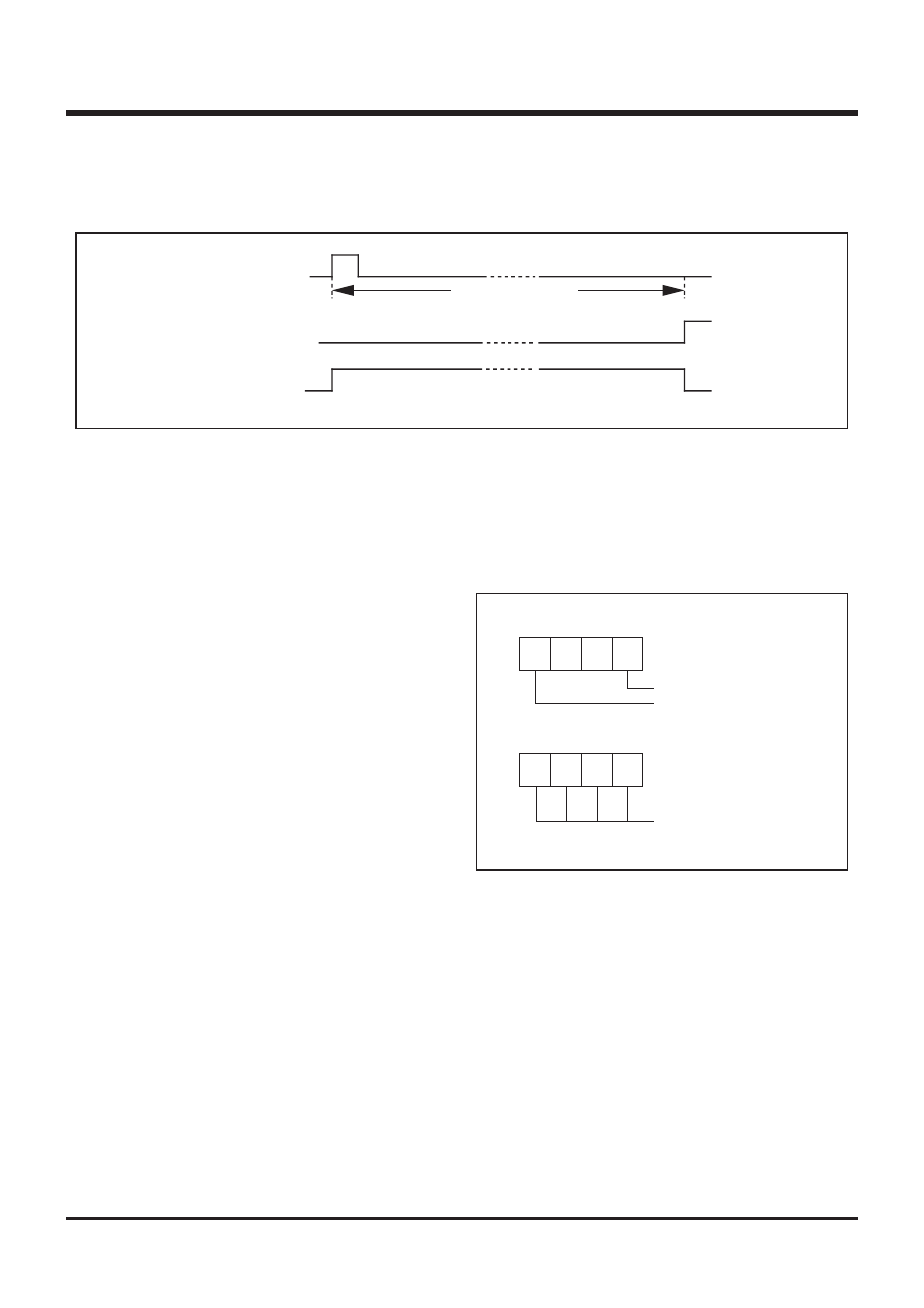
(8) A-D conversion timing chart
Figure 27 shows the A-D conversion timing chart.
Fig. 27 A-D conversion timing chart
(9) How to use A-D conversion
How to use A-D conversion is explained using as example in which
the analog input from P4
0
/A
IN4
pin is A-D conver ted, and the high-
order 4 bits of the converted data are stored in address M(Z, X, Y)
= (0, 0, 0), the middle-order 4 bits in address M(Z, X, Y) = (0, 0, 1),
and the low-order 2 bits in address M(Z, X, Y) = (0, 0, 2) of RAM.
The A-D interrupt is not used in this example.
➀
After selecting the A
IN4
pin function with the bit 0 of the register
Q2, select A
IN4
pin and A-D conversion mode with the register
Q1 (refer to Figure 28).
➁
Execute the ADST instruction and start A-D conversion.
➂
Examine the state of ADF flag with the SNZAD instruction to de-
termine the end of A-D conversion.
➃
Transfer the low-order 2 bits of converted data to the high-order
2 bits of register A (TALA instruction).
➄
Transfer the contents of register A to M (Z, X, Y) = (0, 0, 2).
➅
Transfer the high-order 8 bits of converted data to registers A
and B (TABAD instruction).
➆
Transfer the contents of register A to M (Z, X, Y) = (0, 0, 1).
➇
Transfer the contents of register B to register A, and then, store
into M(Z, X, Y) = (0, 0, 0).
ADST instruction
A-D conversion
completion flag (ADF)
62 machine cycles
DAC operation signal