Clock control, Hardware, Function block operations – Renesas 4514 User Manual
Page 70

4513/4514 Group User’s Manual
HARDWARE
1-57
CLOCK CONTROL
The clock control circuit consists of the following circuits.
• System clock generating circuit
• Control circuit to stop the clock oscillation
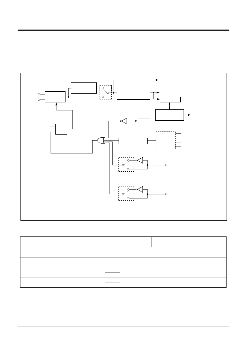
Fig. 41 Clock control circuit structure
Table
23 Clock control register MR
Note : “R” represents read enabled, and “W” represents write enabled.
• Control circuit to switch the middle-speed mode and high-speed
mode
• Control circuit to return from the RAM back-up state
MR
3
MR
2
MR
1
MR
0
Clock control register MR
f(X
IN
) (high-speed mode)
f(X
IN
)/2 (middle-speed mode)
This bit has no function, but read/write is enabled.
This bit has no function, but read/write is enabled.
This bit has no function, but read/write is enabled.
System clock selection bit
Not used
Not used
Not used
at reset : 1000
2
at RAM back-up : 1000
2
0
1
0
1
0
1
0
1
R/W
Instruction clock
MR
3
1
0
RESET
Falling detected
Ports P0
0
, P0
1
Ports P0
2
, P0
3
Ports P1
0
, P1
1
Ports P1
2
, P1
3
Multi-
plexer
K0
0
,K0
1
,K0
2
,K0
3
Counter
Wait time (Note)
control circuit
Software
start signal
R
S
Q
POF instruction
X
IN
X
OUT
I1
2
0
“L” level
1
P3
0
/INT
0
Key-on wake up control register
I2
2
0
1
P3
1
/INT
1
Oscillation
circuit
Division circuit
(divided by 2)
Internal clock
generation circuit
(divided by 3)
“H” level
“L” level
“H” level
Note: The wait time control circuit is used to generate the time required to stabilize the f(X
IN
) oscillation.
System clock
FUNCTION BLOCK OPERATIONS
