2 related registers, Application, 1 i/o pins – Renesas 4514 User Manual
Page 107

2-4
APPLICATION
2.1 I/O pins
4513/4514 Group User’s Manual
(7)
Port D
D
0
–D
7
are eight independent I/O ports.
■
Input/output of port D
Each pin of port D has an independent 1-bit wide I/O function. For I/O of ports D
0
–D
7
, select one
of port D with the register Y of the data pointer first.
●
Data input to port D
Set the output latch of specified port Di (i = 0 to 7) to “1” with the SD instruction.
When the output latch is set to “0,” “L” level is input.
When the SZD instruction is executed, if the port specified by register Y is “0,” the next
instruction is skipped. If it is “1,” the next instruction is executed.
●
Data output from port D
Set the output level to the output latch with the SD and RD instructions.
The state of pin enters the high-impedance state when the SD instruction is executed.
The states of all port D enter the high-impedance state when the CLD instruction is executed.
The state of pin becomes “L” level when the RD instruction is executed.
The output structure is an N-channel open-drain.
Notes 1: When the SD and RD instructions are used, do not set “1000
2
” or more to register Y.
2: Port D
6
is also used as CNTR0, and port D
7
is also used as CNTR1. Accordingly, when
using ports D
6
and D
7
functions, set bit 0 (W6
0
) and bit 2 (W6
2
) of timer control register
W6 to “0.”
2.1.2 Related registers
(1)
Pull-up control register PU0
Register PU0 controls the ON/OFF of the ports P0
0
–P0
3
and P1
0
–P1
3
pull-up transistor.
Set the contents of this register through register A with the TPU0A instruction.
The contents of register PU0 is transferred to register A with the TAPU0 instruction.
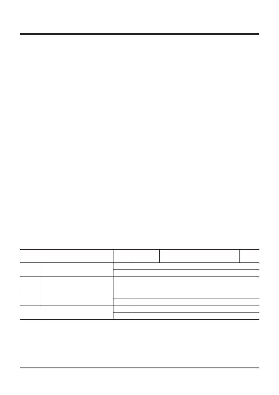
Table 2.1.1 shows the pull-up control register PU0.
Table 2.1.1 Pull-up control register PU0
Pull-up control register PU0
at reset : 0000
2
at RAM back-up : state retained
R/W
Pull-up transistor OFF
Pull-up transistor ON
Pull-up transistor OFF
Pull-up transistor ON
Pull-up transistor OFF
Pull-up transistor ON
Pull-up transistor OFF
Pull-up transistor ON
Ports P1
2
, P1
3
pull-up transistor control bit
Ports P1
0
, P1
1
pull-up transistor control bit
Ports P0
2
, P0
3
pull-up transistor control bit
Ports P0
0
, P0
1
pull-up transistor control bit
0
1
0
1
0
1
0
1
PU0
3
PU0
2
PU0
1
PU0
0
Note: “R” represents read enabled, and “W” represents write enabled.
