2 connection of bypass capacitor across v, Line and v, Line – Renesas 4514 User Manual
Page 193: Appendix, N.g. o.k

3-26
APPENDIX
3.4 Notes on noise
4513/4514 Group User’s Manual
(5) Wiring to V
PP
pin of One Time PROM version
In the built-in PROM version of the 4513/4514
Group, the CNV
SS
pin is also used as the
built-in PROM power supply input pin V
PP
.
●
When the V
PP
pin is also used as the
CNV
SS
pin
Connect an approximately 5 k
Ω
resistor to
the V
PP
pin the shortest possible in series
a n d a l s o t o t h e V
S S
p i n . W h e n n o t
connecting the resistor, make the length of
wiring between the V
PP
pin and the V
SS
pin the shortest possible (refer to Figure
3.4.5)
Note: Even when a circuit which included an
approximately 5 k
Ω
resistor is used in the
Mask ROM version, the microcomputer
operates correctly.
●
Reason
The V
PP
pin of the One Time PROM ver-
sion is the power source input pin for the
built-in PROM. When programming in the
built-in PROM, the impedance of the V
PP
pin is low to allow the electric current for
writing flow into the PROM. Because of
this, noise can enter easily. If noise enters
the V
PP
pin, abnormal instruction codes or
data are read from the built-in PROM, which
may cause a program runaway.
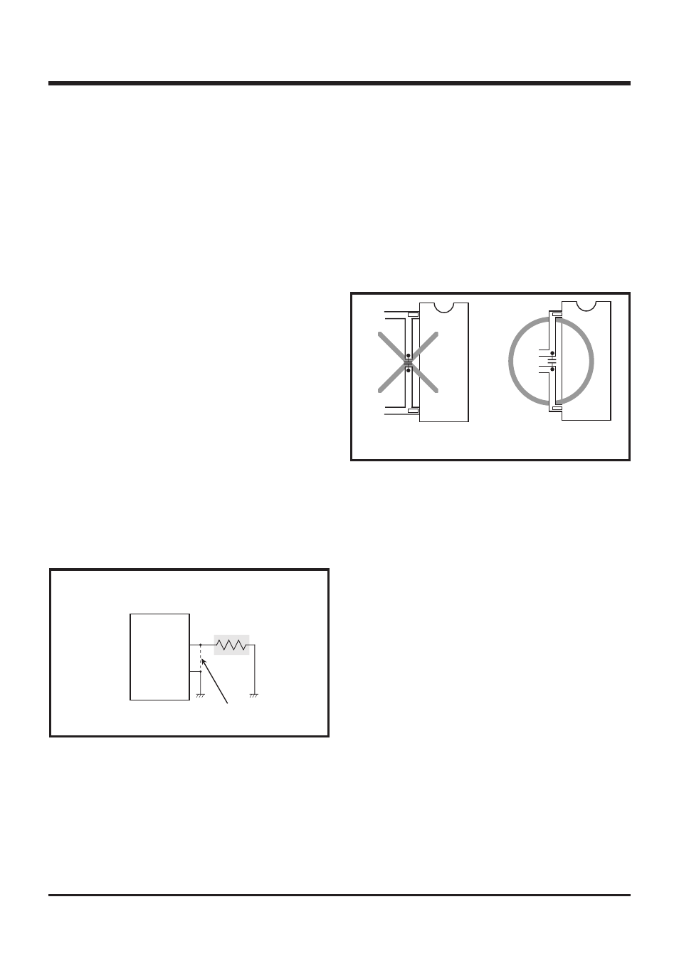
Fig. 3.4.5 Wiring for the V
PP
pin of the One Time
PROM version
CNV
SS
/V
PP
When the V
PP
pin is also used as the CNV
SS
pin
V
SS
In the shortest
distance
Approximately
5k
Ω
3.4.2 Connection of bypass capacitor across V
SS
line and V
DD
line
Connect an approximately 0.1
µ
F bypass capacitor
across the V
SS
line and the V
DD
line as follows:
• Connect a bypass capacitor across the V
SS
pin
and the V
DD
pin at equal length.
• Connect a bypass capacitor across the V
SS
pin
and the V
DD
pin with the shortest possible wiring.
• Use lines with a larger diameter than other signal
lines for V
SS
line and V
DD
line.
• Connect the power source wiring via a bypass
capacitor to the V
SS
pin and the V
DD
pin.
Fig. 3.4.6 Bypass capacitor across the V
SS
line
and the V
DD
line
V
SS
V
DD
V
SS
V
DD
N.G.
O.K.
