Table 1-4. local i/o devices memory map -22 – Motorola MVME1X7P User Manual
Page 48
1-22
Computer Group Literature Center Web Site
Programming Issues
1
($00000000 - $003FFFFF). The VMEchip2 and DRAM map
decoders are disabled by a local bus reset.
On the MVME177P, the Flash/EPROM memory is mapped at
$00000000 - $003FFFFF by hardware default through the
VMEchip2.
2. This area is user-programmable. The suggested use is shown in the
table. The DRAM decoder is programmed in the MCECC chip, and
the local-to-VMEbus decoders are programmed in the VMEchip2.
3. Size is approximate.
4. Cache inhibit depends on devices in area mapped.
5. This area is not decoded. If these locations are accessed and the
local bus timer is enabled, the cycle times out and is terminated by
a TEA signal.
6. The Flash and EEPROM configuration is jointly controlled by a
configuration switch (S4) as described in Chapters 1 and 4 of
MVME177P Single Board Computer Installation and Use, and by
control bit GPIO2 in the VMEchip2 ASIC, as described in
. Depending on the setting of S4, this address space
may reference 2MB EPROM, 1MB EPROM and 2MB Flash, or
4MB Flash.
focuses on the Local I/O Devices portion of the local bus Main
Memory Map..
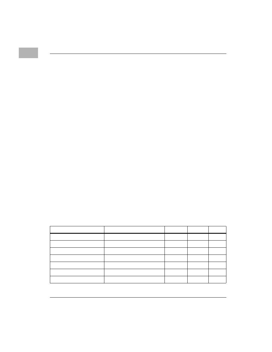
Table 1-4. Local I/O Devices Memory Map
Address Range
Devices Accessed
Port Size
Size
Notes
$FFF00000 - $FFF3FFFF
Reserved
--
256KB
5
$FFF40000 - $FFF400FF
VMEchip2 (LCSR)
D32
256B
1,4
$FFF40100 - $FFF401FF
VMEchip2 (GCSR)
D32-D8
256B
1,4
$FFF40200 - $FFF40FFF
Reserved
--
3.5KB
5,7
$FFF41000 - $FFF41FFF
Reserved
--
4KB
5
$FFF42000 - $FFF42FFF
PCCchip2
D32-D8
4KB
1
$FFF43000 - $FFF430FF
Petra/MCECC #1
D8
256B
1