Motorola MVME1X7P User Manual
Page 45
Functional Description
http://www.motorola.com/computer/literature
1-19
1
Notes
1.
RESET
switch control.
2. Watchdog timer control.
3. Access and watchdog timer parameters.
4. MPU TEA (bus error) status
5. Bit numbering for the VMEchip2 and Petra ASICs has a one-to-one
correspondence.
6.
ABORT
switch interrupt control. Implemented also in the
VMEchip2, but with a different bit organization (refer to the
VMEchip2 description in Chapter 2). In the MVME1X7P, the
ABORT
switch is wired to the Petra chip, not the VMEchip2.
7. The SRAM and EPROM decoder in the VMEchip2 (version 2) must
be disabled by software before any accesses are made to these
address spaces.
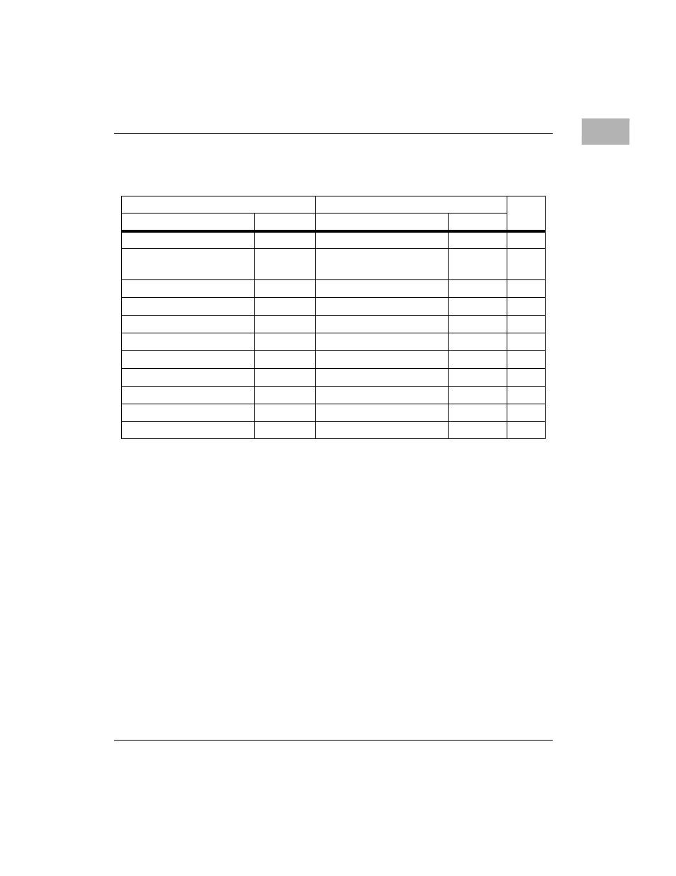
Table 1-2. Functions Duplicated in VMEchip2 and Petra ASICs
VMEchip2
Petra Chip
Notes
Address
Bit #
Address
Bit #
$FFF40060
28-24
$FFF42044
28-24
1,5
$FFF40060
22-19,
17,16
$FFF42044
22-19,
17,16
2,5
$FFF4004C
13-8
$FFF42044
13-8
3,5
$FFF40048
7
$FFF42048
8
4
$FFF40048
9
$FFF42048
9
4,5
$FFF40048
10
$FFF42048
10
4,5
$FFF40048
11
$FFF42048
11
4,5
$FFF40064
31-0
$FFF4204C
3-0
8
$FFF42040
6- 0
6
$FF800000-$FFBFFFFF
31-0
$FF800000-$FFBFFFFF
31-0
7
$FFE00000-$FFEFFFFF
31-0
Programmable
31-0
7