Motorola MVME1X7P User Manual
Page 215
Programming Model
http://www.motorola.com/computer/literature
3-17
3
A normal read access to the Vector Base Register yields the value $0F if
the read happens before it has been initialized. A normal read access yields
all 0s on bits 0-3 and the value that was last written on bits 4-7 if the read
happens after the Vector Base Register has been initialized. A suggested
setting of the Vector Base Register is $50.
The encoding for the interrupt sources is shown below, where IV3-IV0
refer to bits 3-0 of the vector passed during the IACK cycle:
The PCCchip2 supports an auto vector mode for the Cirrus Logic CD2401
SCC serial port. (Refer to the AVEC bit in the following registers: SCC
Modem Interrupt Control Register, SCC Transmit Interrupt Control
Register, and SCC Receive Interrupt Control Register.) If this mode is
disabled by setting the AVEC bits to 0, then the PCCchip2 obtains the
vector from the SCC and passes it to the MPU. Using the auto vector mode
is NOT recommended.
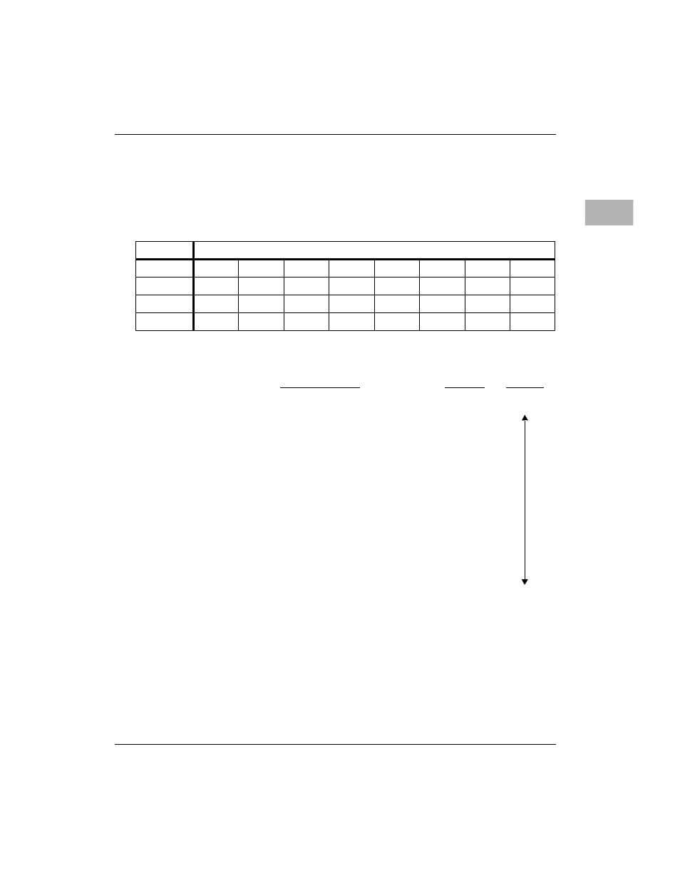
ADR/SIZ
$FFF42003 (8 bits)
BIT
7
6
5
4
3
2
1
0
NAME
IV7
IV6
IV5
IV4
IV3
IV2
IV1
IV0
OPER
R/W
R/W
R/W
R/W
R
R
R
R
RESET
0 PL
0 PL
0 PL
0 PL
1 PL
1 PL
1 PL
1 PL
Interrupt Source
IV3-IV0
Priority
Printer Port-BSY
$0
Lowest
Printer Port-PE
$1
Printer Port-SELECT
$2
Printer Port-FAULT
$3
Printer Port-ACK
$4
SCSI IRQ
$5
LANC ERR
$6
LANC IRQ
$7
Tick Timer 2 IRQ
$8
Tick Timer 1 IRQ
$9
GPIO IRQ
$A
Serial Modem IRQ (auto vector mode only)
$B
Serial RX IRQ (auto vector mode only)
$C
Serial TX IRQ (auto vector mode only)
$D
Highest