Functional description, General description, Functional description -2 – Motorola MVME1X7P User Manual
Page 200: General description -2, Figure 3-1. pccchip2 block diagram -2

3-2
Computer Group Literature Center Web Site
PCCchip2
3
Functional Description
The following sections provide an overview of the functions provided by
the PCCchip2. A detailed programming model for the PCCchip2 control
and status registers is provided in a later section.
General Description
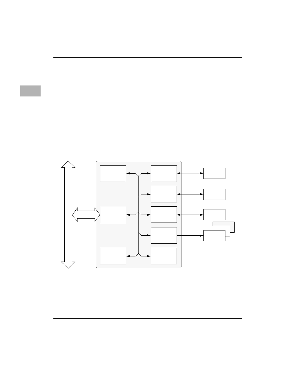
The PCCchip2 interfaces the MC68040 microprocessor bus to the local
peripherals on the Single-Board Computers including: battery-backed
RAM, Serial Communications Controller (CL-CD2401), LAN controller
(82596CA), and SCSI controller (NCR53C710). The PCCchip2 also
provides two 32-bit timers and a parallel I/O port. The block diagram of
the PCCchip2 is shown as Figure 3-1.
Figure 3-1. PCCchip2 Block Diagram
BBRAM
PARALLEL
I/O PORT
CD2401
SCC
TICK
TIMER 1
TICK
TIMER 2
INTERRUPT
HANDLER
BBRAM
I/F
PRINTER
PORT
I/F
CD2401
SERIAL
I/F
MISC.
MAP
DECODER
bd065 9209
SCSI
MEMC040
LANC
MC68040
BUS
I/F
M
C
68
040
B
U
S
- SB5101U DOCSIS 2.0 Cable Modem (16 pages)
- PTP 500 (20 pages)
- Netopia 3347-02-ENT (3 pages)
- SBV5220 (64 pages)
- AP-51XX (698 pages)
- SURFboard SVG2501 Series (34 pages)
- MESH Wireless Router MWR6300 (2 pages)
- MVME712AM (74 pages)
- SURFBOARD SBG1000 (16 pages)
- RSGu3502 (5 pages)
- SURFboard SBG941U (78 pages)
- Netopia 2240N-VGx (5 pages)
- SURFboard SVG2501 (8 pages)
- WR850G (93 pages)
- WR850GP (95 pages)
- USBW 200 (12 pages)
- ONCE SC140 (28 pages)
- Netopia 3300 (368 pages)
- MPC8260 (1006 pages)
- WNS25 (2 pages)
- Netopia 7000 (254 pages)
- Viadux 2000 Subscriber Bridge RC2010 (1 page)
- MVME5100 Series (5 pages)
- ColdFire MCF5282 (766 pages)
- MC9S12C-Family (136 pages)
- CG4500 (36 pages)
- SBG900 (130 pages)
- SURFBOARD SB5100 (2 pages)
- SURFboard SB6180 (20 pages)
- SURFBOARD SBG900 (16 pages)
- SURFboard SVG1501U (83 pages)
- SB5100 (74 pages)
- T3 (2 pages)
- H375 (5 pages)
- NETOPIA 2247/57-62 (22 pages)
- SBV5120 (56 pages)
- SBV5120 (57 pages)
- RG2200 (88 pages)
- CME-12B/BC (18 pages)
- SURFboard 574823-001-a (2 pages)
- SURFboard Cable Modem (66 pages)
- CME-12D60 (19 pages)
- DIGITAL VOICE MODEM SBV5122 (24 pages)
- SB4000 (2 pages)
- Canopy FSK and OFDM radios PTP 200 (OFDM (56 pages)
