Vmechip2 revision register, Vmechip2 revision register -103, Table 2-5. vmechip2 memory map (gcsr summary) -103 – Motorola MVME1X7P User Manual
Page 193
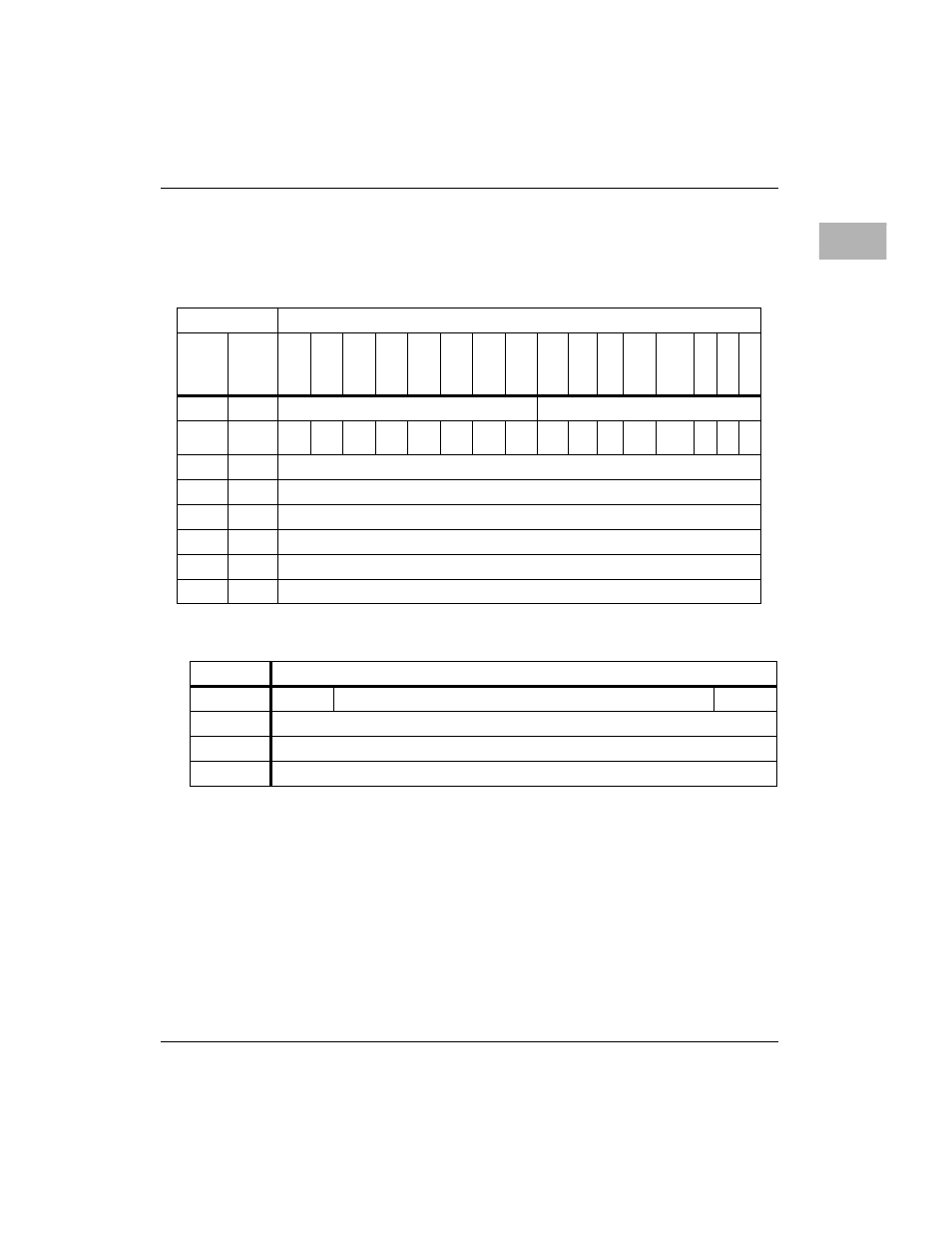
GCSR Programming Model
http://www.motorola.com/computer/literature
2-103
2
shows a summary of the GCSR.
VMEchip2 Revision Register
This register is the VMEchip2 revision register. The revision level for the
VMEchip2 starts at 0 and is incremented if mask changes are required. The
VMEchip2 used on the MVME1x7P is revision $01 or greater.
Table 2-5. VMEchip2 Memory Map (GCSR Summary)
VMEchip2 GCSR Base Address = $FFF40100
Offsets
Bit Numbers
VM
E
bus
Loca
l Bus
15
14
13
12
11
10
9
8
7
6
5
4
3
2
1
0
0
0
Chip Revision
Chip ID
2
4
LM
3
LM
2
LM
1
LM
0
SI
G3
SI
G2
SI
G1
SI
G0
RS
T
IS
F
B
F
SCO
N
SYSF
L
X X X
4
8
General Purpose Control and Status Register 0
6
C
General Purpose Control and Status Register 1
8
10
General Purpose Control and Status Register 2
A
14
General Purpose Control and Status Register 3
C
18
General Purpose Control and Status Register 4
E
1C
General Purpose Control and Status Register 5
ADR/SIZ
Local Bus: $FFF40100/VMEbus: $XXY0 (8 bits)
BIT
15
. . .
8
NAME
VMEchip2 Revision Register
OPER
R
RESET
01 PS