Data control register, Data control register -17 – Motorola MVME1X7P User Manual
Page 265

Programming Model
http://www.motorola.com/computer/literature
4-17
4
Note
This register is configured only during power-up-reset and is
unchanged by software or local reset.
Data Control Register
RWCKB
READ/WRITE CHECKBITS, when set, enables the data
from the seven checkbits in the Petra MCECC sector (bits
30-24) to be written and read on the local MC680x0 data
bus. This bit should be cleared for normal system
operation.
Note that if test software forces a single-bit error to a
location (line) using this function, the scrubber may
correct the location before the test software gets a chance
to check for the single-bit error at that location. This can
be avoided by disabling scrubbing and making sure that
all previous scrubs have completed before performing the
test. Also note that writing bad checkbits can set the
ERRLOG bit in the Error Logger register.
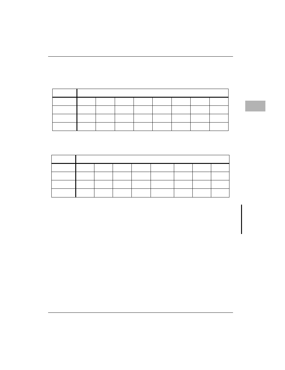
ADR/SIZ
1st $FFF4301C/2nd $FFF4311C (8-bits)
BIT
31
30
29
28
27
26
25
24
NAME
BCK7
BCK6
BCK5
BCK4
BCK3
BCK2
BCK1
BCK0
OPER
R/W
R/W
R/W
R/W
R/W
R/W
R/W
R/W
RESET
0 P
0 P
0 P
1 P
1 P
0 P
0 P
1P
ADR/SIZ
1st $FFF43020/2nd $FFF43120 (16-bits)
BIT
31
30
29
28
27
26
25
24
NAME
0
0
DERC
ZFILL
RWCKB
0
0
0
OPER
R
R
R/W
R/W
R/W
R
R
R
RESET
X
X
1 PLS
0 PLS
0 PLS
X
X
X
