Base address register, Dram control register, 4base address register – Motorola MVME1X7P User Manual
Page 263
Programming Model
http://www.motorola.com/computer/literature
4-15
4
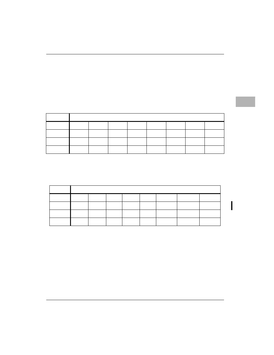
Base Address Register
These eight bits are combined with the two most significant bits in Register
7 (the next register) to form BAD31-BAD22, which defines the base
address of the memory. For larger memory sizes, the lower significant bits
are ignored.
The bit assignments for the Base Address register are:
DRAM Control Register
The bit assignments for the DRAM Control register are:
RAMEN
RAM Enable. This control bit is used to enable the local
bus to perform read/write accesses to the memory.
Accesses are enabled when this bit is set and are disabled
when this bit is cleared. This bit should only be set after
BAD31-BAD22 have been initialized.
ADR/SIZ
1st $FFF43014/2nd $FFF43114 (8-bits)
BIT
31
30
29
28
27
26
25
24
NAME
BAD31
BAD30
BAD29
BAD28
BAD27
BAD26
BAD25
BAD24
OPER
R/W
R/W
R/W
R/W
R/W
R/W
R/W
R/W
RESET
0 PLS
0 PLS
0 PLS
0 PLS
0 PLS
0 PLS
0 PLS
0 PLS
ADR/SIZ
1st $FFF43018/2nd $FFF43118 (8-bits)
BIT
31
30
29
28
27
26
25
24
NAME
BAD23 BAD22 RWB5 RWB4
RWB3 NCEIEN
NCEBEN
RAMEN
OPER
R/W
R/W
R/W
R/W
R/W
R/W
R
R/W
RESET
0 PLS
0 PLS
0 PLS
0 PLS
0 PLS
0 PLS
0 PLS
0 PLS