FUJITSU CAN-Motor Board MB91F267N User Manual
Page 72
AN07-00180-3E
- 72 -
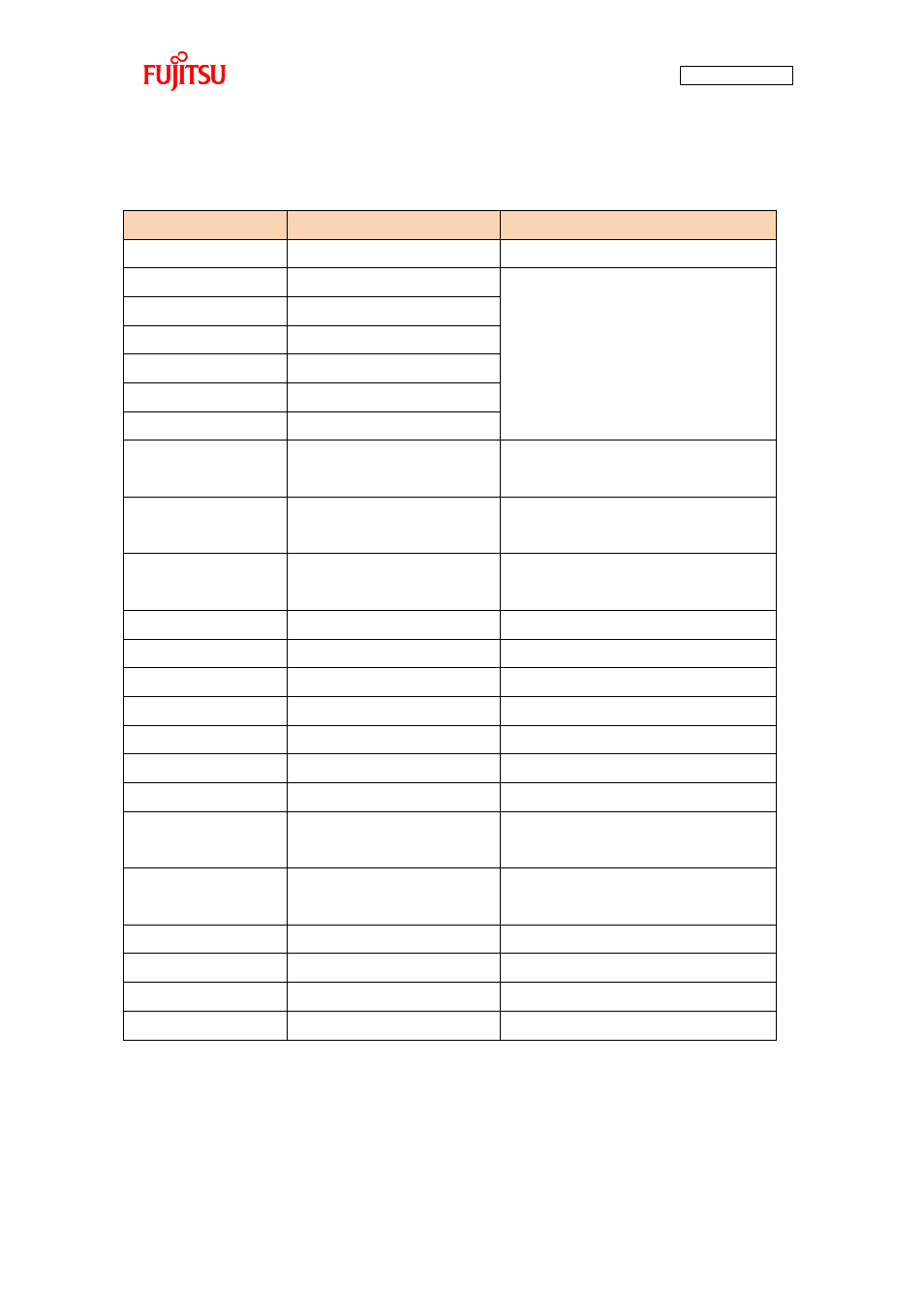
Table 4-4 Description of the output compare registers and setting values
Register name
Setting value [function]
Description
CPCLRB0
1599
Compare value setting
OCCPB0
1598
Output compare value settings
OCCPB1
1000
OCCPB2
1598
OCCPB3
1000
OCCPB4
1598
OCCPB5
1000
OCMOD
0xFF [1 output on a match]
Designation of the operation on a compare
match
OCSH1,3,5_BTS1
1 [transfer on a compare clear
match]
Buffer transfer select bit (ch 1,3,5)
OCSH1,3,5_BTS0
1 [transfer on a compare clear
match]
buffer transfer select bit (ch 0,2,4)
OCSH1,3,5_CMOD
1 [ inversion mode]
Output level inversion mode bit
OCSH1,3,5_OTE1
0 [general-purpose output port]
Output enable bit (ch 1,3,5)
OCSH1,3,5_OTE0
0 [general-purpose output port]
Output enable bit (ch 0,2,4)
OCSH1,3,5_OTD1
0 [1 output]
Output level bit (ch 1,3,5)
OCSH1,3,5_OTD0
0 [1 output]
Output level bit (ch 0,2,4)
OCSL0,2,4_IOP1
0 [bit clear]
Compare match interrupt flag bit (ch 1,3,5)
OCSL0,2,4_IOP0
0 [bit clear]
Compare match interrupt flag bit (ch 0,2,4)
OCSL0,2,4_IOE1
0
[compare
match
interrupt
disable]
Compare match interrupt enable bit (ch 1,3,5)
OCSL0,2,4_IOE0
0
[compare
match
interrupt
disable]
Compare match interrupt enable bit (ch 0,2,4)
OCSL0,2,4_BUF1
0 [compare buffer enable]
Compare buffer disable bit (ch 1,3,5)
OCSL0,2,4_BUF0
0 [compare buffer enable]
Compare buffer disable bit (ch 0,2,4)
OCSL0,2,4_CST1
0 [compare operation disable]
Compare operation enable bit (ch 1,3,5)
OCSL0,2,4_CST0
1 [compare operation enable]
Compare operation enable bit (ch 0,2,4)