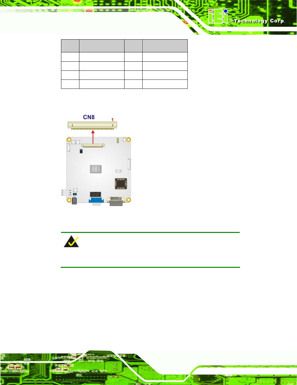
12 power output connector, Figure 4-32: lvds output connector location, Table 4-37: lvds output connector pinouts – IEI Integration DM_Series v1.14 User Manual
Page 115: Dm series industrial monitor page 115

DM Series Industrial Monitor
Page
115
PIN
DESCRIPTION
PIN
DESCRIPTION
23
TXE0+
24
TXE0-
25
GND
26
GND
27
VDD
28
VDD
29
VDD
30
VDD
Table 4-37: LVDS Output Connector Pinouts
Figure 4-32: LVDS Output Connector Location
NOTE:
The supply voltage (3.3V (Default), 5V or 12V) can be selected via JP1.
4.4.12 Power Output Connector
CN Label:
CN12, CN13
CN Type:
2-pin wafer connector
CN Pinouts:
CN Location:
