Toshiba – Toshiba TMP87CP24AF User Manual
Page 95
Attention! The text in this document has been recognized automatically. To view the original document, you can use the "Original mode".
TOSHIBA
TMP87CM24A/P24A
(3)
Booster circuit for LCD driver
The
TMP87CM24A/P24A
incorporate
a
booster
circuit
for
the
LCD
driver
(IV
x
3
times)
so
that
the
LCD display does not flicker due to fluctuations in the power supply voltage.
The
booster
circuit
boosts
the
output
voltage
for
the
segment/common
signal
by
double
(VLCD2)
and triple (VLCD3) in relation to the on-chip output voltage (1V typ).
Figure
2-46
shows
an
example
of
a
booster
circuit
for
the
LCD
driver.
It
takes
to
maximum
1
s
(Topr=
-10°C)
for
the
booster
circuit
to
reach
the
specified
voltage
at
return
from
reset
or
standby.
If
the
LCD
circuit
is
enabled
before
the
specified
voltage
is
reached
boosting
takes
longer.
The
reference
frequency
of
the
booster
circuit
at
initialization
is
1
kHz.
Selecting
the
frequency
using
the
SLFR
in
the
command
register
(LCDCR)
raises
the
drive
capability
of
segment/common.
Table 2-10 shows the reference frequency of the booster circuit.
TMP87CM24A/P24A
V3
V2
VI
Cl
CO
7^
C = 0.1 to0.47//F
Figure 2-46. Example of a Booster Circuit
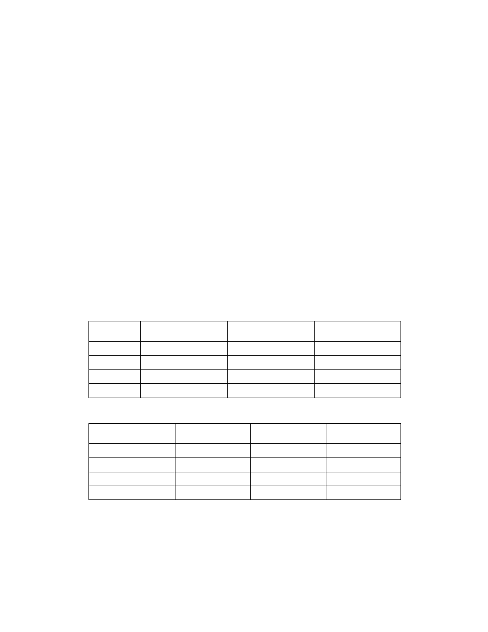
Table 2-10. Reference Frequency of the Booster Circuit
SLFR
Frequency
fc =
8
MHz
fs = 32.768 kHz
00
fc/213 orfs/25
0.98 kHz
1.02 kHz
01
fc/211 orfs/23
3.91 kHz
4.09 kHz
10
fc
/210
orfs
/22
7.81 kHz
8.19 kHz
11
fc/29
15.63 kHz
—
Table 2-11. Selection of V3 Boosting Frequency
Boosting frequency
fc = 8MHz
fc = 4MHz
fc = 32.768 MHz
fc/213 orfs/25
40 ms
80 ms
40 ms
fc/211 or fs/23
10 ms
20 ms
10 ms
fc/210 or fs/24
5 ms
10 ms
5 ms
fc/29
2.5 ms
5 ms
—
Л/oie
7;
Торг
=
25
X,
0.1
juF^
0.47juF
Note 2:
V3 booting time at VDD is stable.
3
-
24-95
2002
-
10-03