Operational description 1. cpu core functions, 1 memory address map, Toshiba – Toshiba TMP87CP24AF User Manual
Page 6
Attention! The text in this document has been recognized automatically. To view the original document, you can use the "Original mode".

TOSHIBA
TMP87CM24A/P24A
Operational Description
1. CPU Core Functions
The CPU core consists of a CPU, a system clock controller, an interrupt controller, and a watchdog timer.
This section provides a description of the CPU core, the program memory (ROM), the data memory
(RAM), and the reset circuit.
1.1
Memory Address Map
TheTLCS-870
Series
is
capable
of
addressing
64K
bytes
of
memory.
Figure
1-1
shows
the
memory
address
mapsof
theTMP87CM24A/P24A.
In
theTLCS-870
Series,
the
memory
is
organized
4
address
spaces
(ROM,
RAM,
SFR,
and
DBR).
It
uses
a
memory
mapped
I/O
system,
and
all
I/O
registers
are
mapped
in
the
SFR/DBR
address
spaces.
There
are
16
banks
of
general-purpose
registers.
The
register
banks
are
also
assigned to the first 128 bytes of the RAM address space.
SFR
OOOO
h
003F
^ 0040
OOBF
OOCO
RAM
64 bytes
128 bytes
1920 bytes
DBR
ROM
083 F
/ 0F80
k OFFF
4000
FFOO
FFBF
FFCO
FFDF
FFEO
\ FFFF
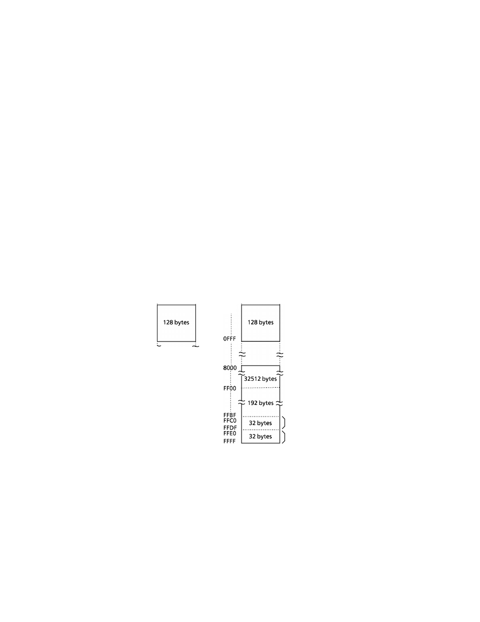
48896 bytes
192 bytes
32 bytes
32 bytes
TMP87CP24A
OOOO
h
003F
0040
OOBF
OOCO
083 F
0F80
64 bytes
128 bytes
1920 bytes
Register banks
(8 registers x16 banks)
ROM:
Read Only Memory includes:
Program memory
RAM:
Random Access Memory includes :
Data memory
Stack
General-purpose register banks
SFR:
Special Function Register includes:
I/O ports
Peripheral control registers
Peripheral status registers
System control registers
Interrupt control registers
Program Status Word
DBR:
Data Buffer Register includes:
SIO data buffer
TMP87CM24A
Vector table for vector call
instructions (16 vectors)
Vector table for interrupts/
reset (16 vectors)
/
Entry area for
page call
instructions
Figure 1-1. Memory Address Maps
3
-
24-6
2002
-
10-03
