Electrical characteristics, Ov ), Toshiba – Toshiba TMP87CP24AF User Manual
Page 112
Attention! The text in this document has been recognized automatically. To view the original document, you can use the "Original mode".
TOSHIBA
TMP87CM24A/P24A
Electrical Characteristics
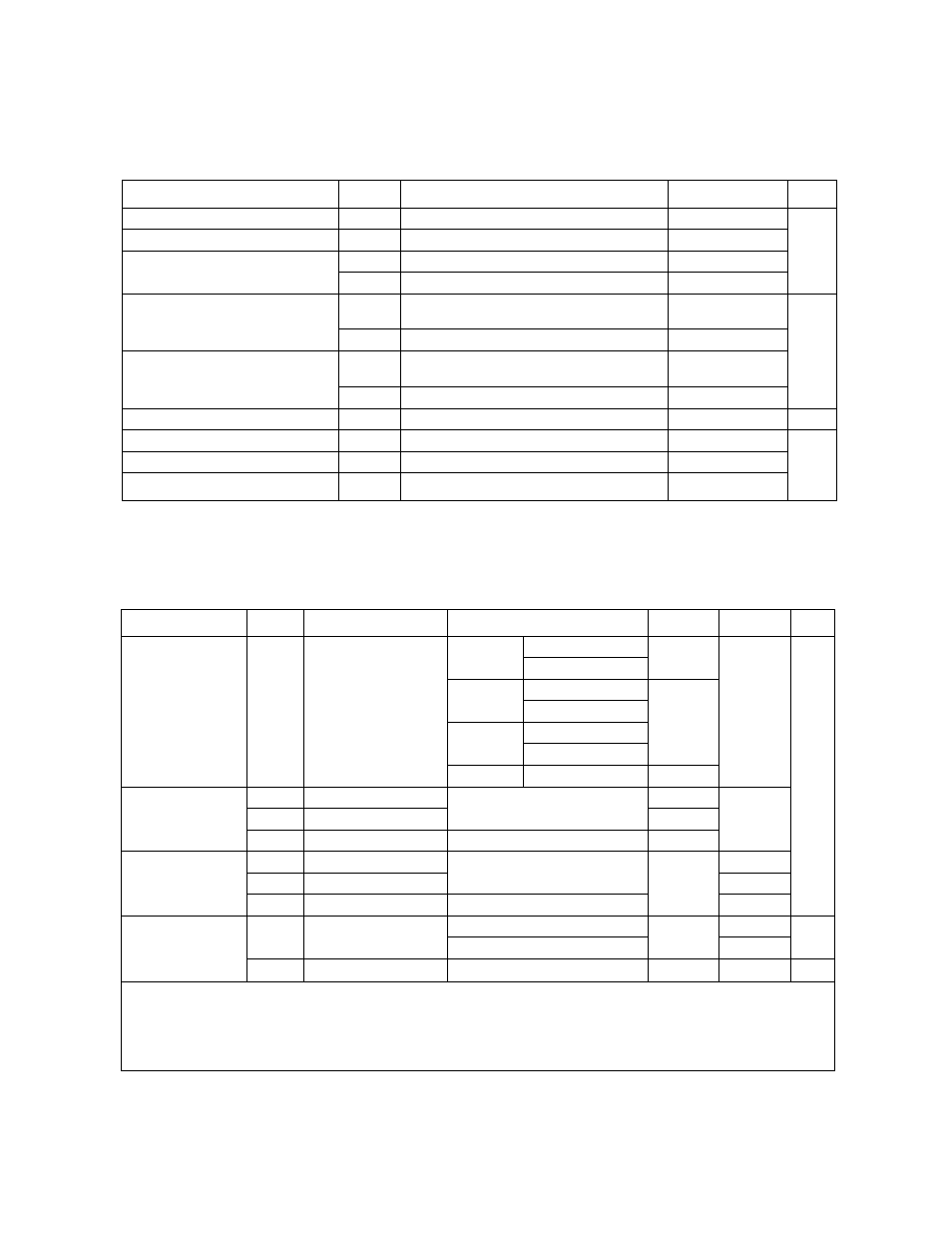
Absolute Maximum Ratings
(Vss =
ov )
Parameter
Symbol
Pins
Ratings
Unit
Supply Voltage
V
dd
- 0.3 to 6.5
V
Input Voltage
V|N
— 0.3 to V
qd
+ 0.3
Output Voltage
VouTi
Except P20 and P3 ports
— 0.3 to V
qd
+ 0.3
V
q
UT2
Ports P20, P3
- 0.3 to 5.5
Output Current (Per 1 pin)
I
quti
Ports PO, PI, P2, P3, P5, P6, P7, P8, P9, P4
(except P41)
3.2
mA
loUT2
P41
30
Output Current (Total)
2 I
quti
Ports PO, PI, P2, P3, P5, P6, P7, P8, P9, P4
(except P41)
120
2 I
qut
2
P41
30
Power Dissipation
[Торг
= 70°C]
PD
350
mW
Soldering Temperature (time)
Tsid
260 (10 s)
°C
Storage Temperature
Tstg
-55 to 125
Operating Temperature
Торг
- lOto70
Note: The
absolute maximum ratings are rated
values
which must not be exceeded
during operation,
even for
an instant
Any
one of the ratings must not be exceeded. If any absolute maximum rating is exceeded, a device may break down or its
performance may be degraded, causing it to catch fire or explode resulting in injury to the user. Thus, when designing
products which include this device, ensure that no absolute maximum rating value will ever be exceeded.
Recommended Operating Conditions
(Vss = 0 V, Торг = - 10 to 70°C)
Parameter
Symbol
Pins
Conditions
Min
Max
Unit
fc = 8MHz
NORMAL1,2mode
4.5
IDLE1,2 mode
fc = 4.2MHz
NORMAL1,2mode
Supply Voltage
V
dd
IDLE1,2 mode
2.2
5.5
fs =
SLOW mode
32.768 kHz
SLEEP mode
STOP mode
2.0
V
V|Hi
Except hysteresis input
V
X
0.70
Input High Voltage
V|H2
Hysteresis input
VDD=‘t--> V
V
ddx
O.75
V
dd
V|H3
V
dd
<4.5V
V
X
0.90
V|L1
Except hysteresis input
V
X
0.30
Input Low Voltage
V|L2
Hysteresis input
VDD=‘t--> V
0
V
qqx
O.25
V|L3
V
dd
<4.5V
V
X 0.1 0
fc
XIN, XOUT
V
dd
= 4.5 to 5.5 V
0.4
8.0
MHz
Clock Frequency
V
dd
= 2.2 to 5.5 V
4.2
fs
XTIN, XTOUT
30.0
34.0
kHz
Note 1: The recommended operating conditions for a device are operating conditions under which it can be guaranteed that
the device will operate as specified. If the device is used under operating conditions other than the recommended
operating conditions (supply voltage, operating temperature range, specified ACIDC values etc.), malfunction may
occur.
Thus,
when
designing
products
which
include
this
device,
ensure
that
the
recommended
operating
conditions
for the device are always adhered to.
Note 2: Clock frequency fc: Supply voltage range is specified in NORMAL 1/2 mode and IDLE 1/2 mode.
3
-
24-112
2002
-
10-03