Un_jn_jn_jn_n_nlnlr, Toshiba – Toshiba TMP87CP24AF User Manual
Page 84
Attention! The text in this document has been recognized automatically. To view the original document, you can use the "Original mode".
TOSHIBA
TMP87CM24A/P24A
Motel: Tf frame time,
T
q
: data transfer time
^pin
Un_Jn_Jn_Jn_n_nLnLr
ULT
Tf
Note 2:
Note 3:
Note
4:
Note
5:
Note 6:
Note 7:
The lower 4 bits of each buffer are used during 4-bit transfers. Zeros (0) are stored to the upper 4bits
when receiving.
Transmitting
starts
at
the
lowest
address.
Received
data
are
also
stored
starting
from
the
lowest
address to the highest address. For example, in the case of SI01, the first buffer address transmitted is
OFFO
h
.
The value to be loaded to BUF is held after transfer is completed.
SI01CR2/SI02CR2 must be set when the serial interface is stopped (SlOF = 0).
SI01CR2/SI02CR2
are
write-only
registers,
which
cannot
access
any
of
read-modify-write
instructions
such as bit operate, etc.
*: Don't care
Figure 2-34. SIO Control Registers and Status Registers
(1)
Serial Clock
a. Clock Source
SCK (bits 2 to 0 in SI01CR1/SI02CR1) is able to select the following:
© Internal Clock
Any
of
four
frequencies
can
be
selected.
The
serial
clock
is
output
to
the
outside
on
the
SCK1/SCK2 pin. The SCK pin goes high when transfer starts.
When
data
writing
(in
the
transmit
mode)
or
reading
(in
the
receive
mode
or
the
transmit/receive
mode)
cannot
keep
up
with
the
serial
clock
rate,
there
is
a
wait
function
that
automatically
stops
the
serial
clock
and
holds
the
next
shift
operation
until
the
read/write processing is completed.
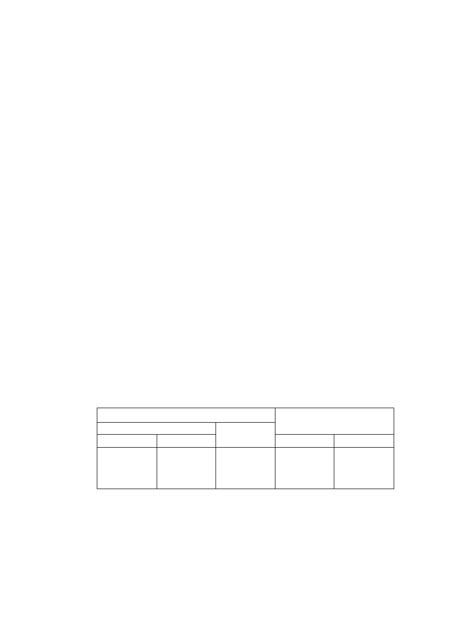
Table 2-8. Serial Clock Rate
Serial clock
Maximum transfer rate
NORMAL1/2, DLE1/2mode
SLOW, SLEEP mode
DV7CK = 0
DV7CK= 1
Atfc = 8MHz
At fs = 32.768 kHz
fc/2’^ [Hz]
fs/2= [Hz]
fs/2= [Hz]
0.954 kbit/s
1 kbit/s
fc/2»
fc/2»
-
30.5
-
fc/2®
fc/2®
-
122
-
fc/2=
fc/2=
-
244
-
Note: 1 Kbit = 1024 bit
3
-
24-84
2002
-
10-03