2 memory interface signals – AMD Geode SC2200 User Manual
Page 50
54
AMD Geode™ SC2200 Processor Data Book
32580B
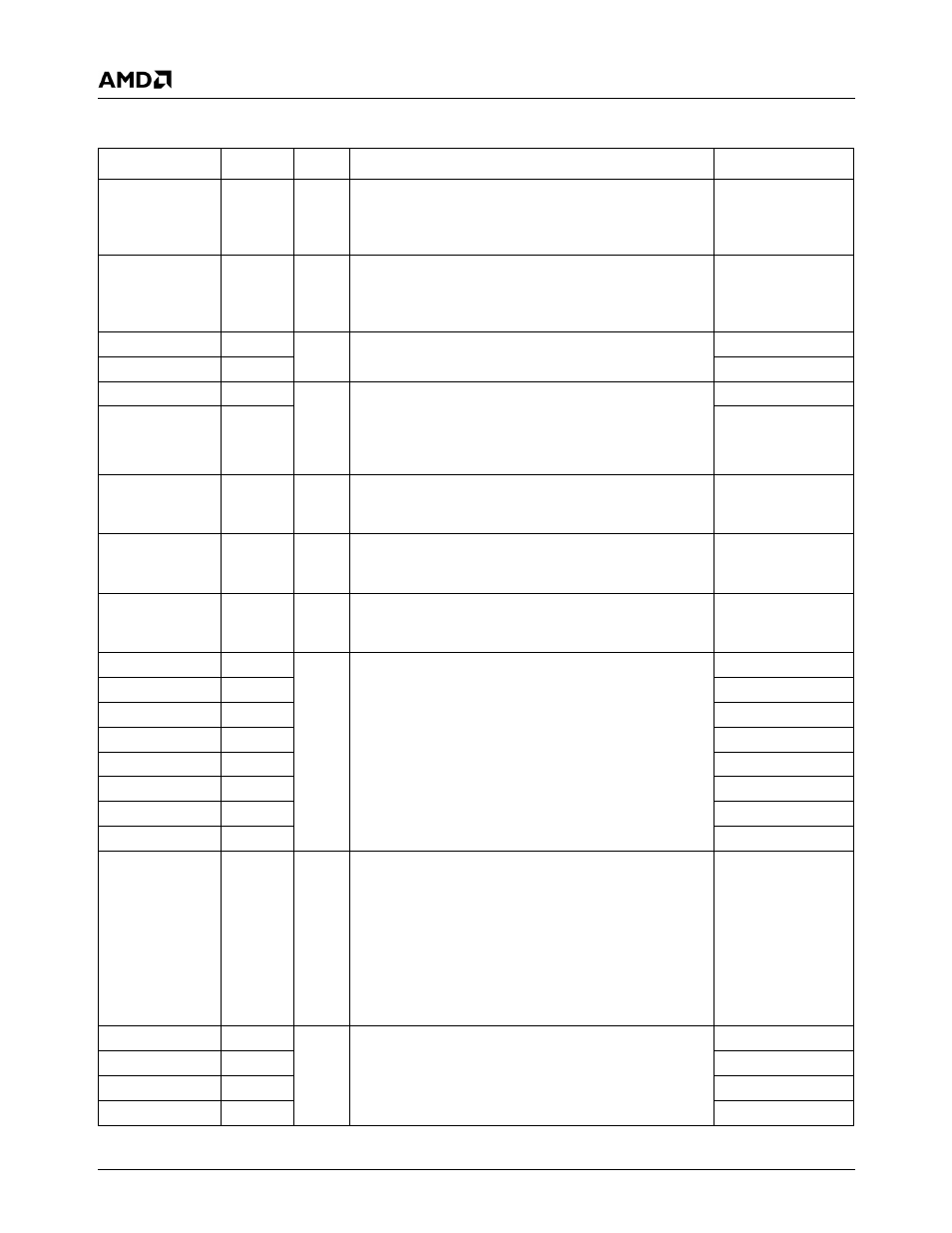
3.4.2
Memory Interface Signals
Signal Name
Ball No.
Type
Description
Mux
MD[63:0]
See
I/O
Memory Data Bus. The data bus lines driven to/from
system memory.
---
MA[12:0]
See
O
Memory Address Bus. The multiplexed row/column
address lines driven to the system memory. Supports
256-Mbit SDRAM.
---
BA1
AK14
O
Bank Address Bits. These bits are used to select the
component bank within the SDRAM.
---
BA0
AJ13
---
CS1#
AH27
O
Chip Selects. These bits are used to select the module
bank within system memory. Each chip select corre-
sponds to a specific module bank. If CS# is high, the
bank(s) do not respond to RAS#, CAS#, and WE# until
the bank is selected again.
---
CS0#
AL12
---
RASA#
AK12
O
Row Address Strobe. RAS#, CAS#, WE# and CKE are
encoded to support the different SDRAM commands.
RASA# is used with CS[1:0]#.
---
CASA#
AJ12
O
Column Address Strobe. RAS#, CAS#, WE# and CKE
are encoded to support the different SDRAM commands.
CASA# is used with CS[1:0]#.
---
WEA#
AH12
O
Write Enable. RAS#, CAS#, WE# and CKE are encoded
to support the different SDRAM commands. WEA# is
used with CS[1:0]#.
---
DQM7
AB31
O
Data Mask Control Bits. During memory read cycles,
these outputs control whether SDRAM output buffers are
driven on the MD bus or not. All DQM signals are
asserted during read cycles.
During memory write cycles, these outputs control
whether or not MD data is written into SDRAM.
DQM[7:0] connect directly to the [DQM7:0] pins of each
DIMM connector.
---
DQM6
AG29
---
DQM5
AK21
---
DQM4
AL15
---
DQM3
AC31
---
DQM2
AG30
---
DQM1
AH23
---
DQM0
AL11
---
CKEA
AL22
O
Clock Enable. These signals are used to enter Suspend/
power-down mode. CKEA is used with CS[1:0]#.
If CKE goes low when no read or write cycle is in
progress, the SDRAM enters power-down mode. To
ensure that SDRAM data remains valid, the self-refresh
command is executed. To exit this mode, and return to
normal operation, drive CKE high.
These signals should have an external pull-down resistor
of 33 K
Ω.
---
SDCLK3
V29
O
SDRAM Clocks. SDRAM uses these clocks to sample
all control, address, and data lines. To ensure that the
Suspend mode functions correctly, SDCLK3 and
SDCLK1 should be used with CS1#. SDCLK2 and
SDCLK0 should be used together with CS0#.
---
SDCLK2
AA28
---
SDCLK1
W29
---
SDCLK0
AJ21
---