1 ball assignments, Table 3-1, Signal definitions legend – AMD Geode SC2200 User Manual
Page 27: Section 3.1 "ball assignments": pro
AMD Geode™ SC2200 Processor Data Book
27
Signal Definitions
32580B
3.1
Ball Assignments
The SC2200 is highly configurable as illustrated in Figure
3-1 on page 25. Strap options and register programming
are used to set various modes of operation and specific
signals on specific balls. This section describes which sig-
nals are available on which balls and provides configuration
information:
• Figure 3-2 on page 28: Illustrates the BGU481 ball
assignments.
• Table 3-2 on page 29: Lists signals according to ball
number. Power Rail, Signal Type, Buffer Type and,
where relevant, Pull-Up or Pull-Down resistors are indi-
cated for each ball in this table. For multiplexed balls, the
necessary configuration for each signal is listed as well.
• Table 3-3 on page 41: Quick reference signal list sorted
alphabetically - listing all signal names and ball
numbers.The tables in this chapter use several common
abbreviations. Table 3-1 lists the mnemonics and their
meanings
Notes:
1)
For each GPIO signal, there is an optional pull-up
resistor on the relevant ball. After system reset, the
pull-up is present.
This pull-up resistor can be disabled via registers in
the Core Logic module. The configuration is without
regard to the selected ball function (except for
GPIO12, GPIO13, and GPIO16). Alternate functions
for GPIO12, GPIO13, and GPIO16 control pull-up
resistors.
For more information, see Section 6.4.1 "Bridge,
GPIO, and LPC Registers - Function 0" on page 198.
2)
Configuration settings listed in this table are with
regard to the Pin Multiplexing Register (PMR). See
Section 4.2 "Multiplexing, Interrupt Selection, and
Base Address Registers" on page 76 for a detailed
description of this register.
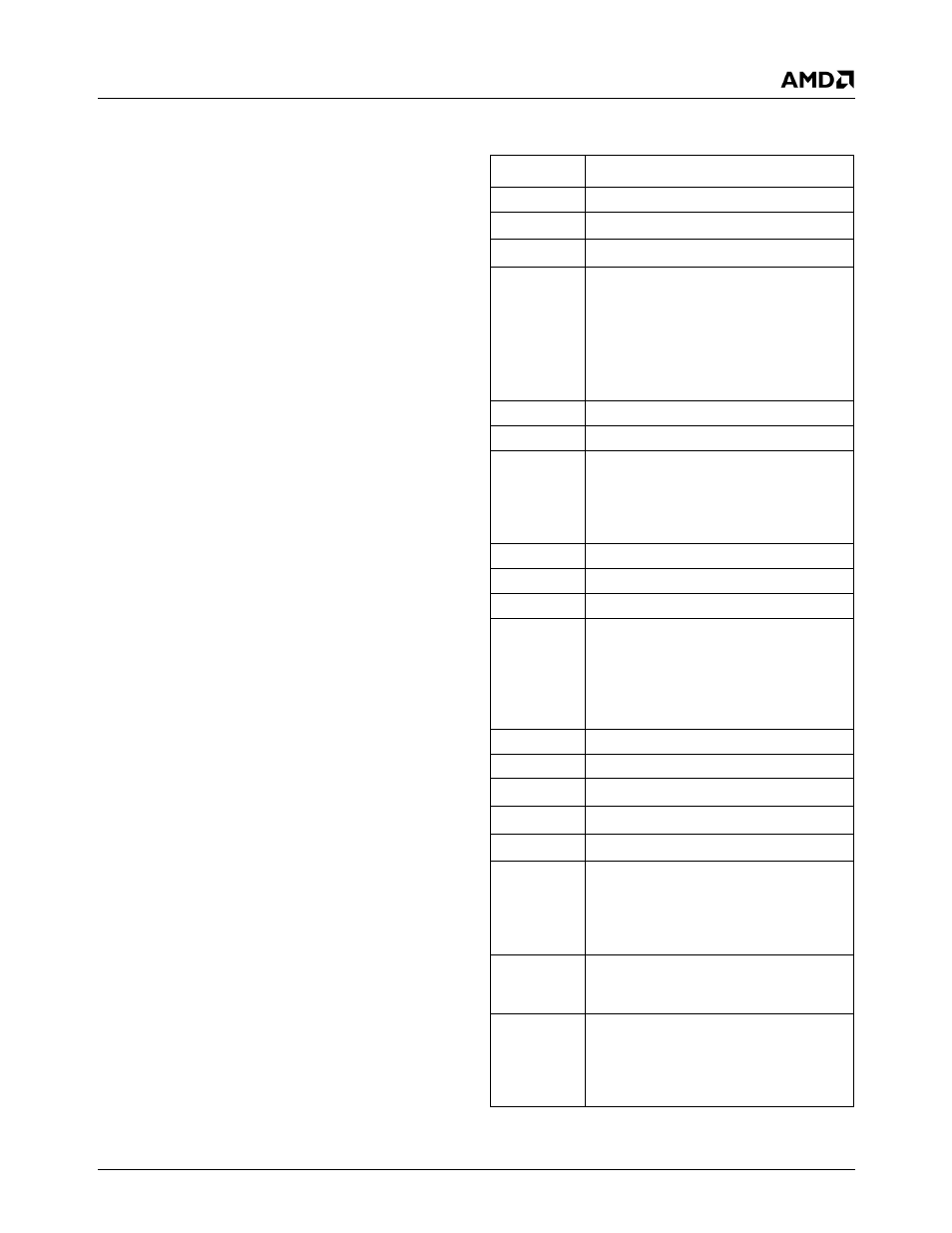
Table 3-1. Signal Definitions Legend
Mnemonic
Definition
A
Analog
AV
SS
Ground ball: Analog
AV
CC
Power ball: Analog
GCB
General Configuration Block registers.
Refer to Section 4.0 "General Configura-
tion Block" on page 75.
Location of the General Configuration
Block cannot be determined by software.
See the AMD Geode™ SC2200 Proces-
sor Specification Update.
I
Input ball
I/O
Bidirectional ball
MCR[x]
Miscellaneous Configuration Register
Bit x: A register, located in the GCB.
Refer to Section 4.1 "Configuration
Block Addresses" on page 75 for further
details.
O
Output ball
OD
Open-drain
PD
Pull-down in K
Ω
PMR[x]
Pin Multiplexing Register Bit x: A regis-
ter, located in the GCB, used to config-
ure balls with multiple functions. Refer to
Section 4.1 "Configuration Block
Addresses" on page 75 for further
details.
PU
Pull-up in K
Ω
TS
TRI-STATE
V
CORE
Power ball: 1.2V
V
IO
Power ball: 3.3V
V
SS
Ground ball
#
The # symbol in a signal name indicates
that the active or asserted state occurs
when the signal is at a low voltage level.
Otherwise, the signal is asserted when
at a high voltage level.
/
A / in a signal name indicates both func-
tions are always enabled (i.e., cycle mul-
tiplexed).
+
A + in signal name indicates the function
is available on the ball, but that either
strapping options or register program-
ming is required to select the desired
function.