6 rom interface, 7 pci and sub-isa signal cycle multiplexing, Table 6-3 – AMD Geode SC2200 User Manual
Page 151: Cycle multiplexed pci / sub-isa balls
AMD Geode™ SC2200 Processor Data Book
159
Core Logic Module
32580B
6.2.5.6
ROM Interface
The Core Logic module positively decodes memory
addresses 000F0000h-000FFFFFh (64 KB) and
FFFC0000h-FFFFFFFFh (256 KB) at reset. These memory
cycles cause the Core Logic module to claim the cycle, and
generate an ISA bus memory cycle with ROMCS#
asserted. The Core Logic module can also be configured to
respond to memory addresses FF000000h-FFFFFFFFh
(16 MB) and 000E0000h-000FFFFFh (128 KB).
8- or 16-bit wide ROM is supported. BOOT16 strap deter-
mines the width after reset. MCR[14,3] (Offset 34h) in the
General Configuration Block (see Table 4-2 on page 76 for
bit details) allows program control of the width.
Flash ROM is supported in the Core Logic module by
enabling the ROMCS# signal on write accesses to the
ROM region. Normally only read cycles are passed to the
ISA bus, and the ROMCS# signal is suppressed for write
cycles. When the ROM Write Enable bit (F0 Index 52h[1])
is set, a write access to the ROM address region causes a
write cycle to occur with MEMW#, WR# and ROMCS#
asserted.
6.2.5.7
PCI and Sub-ISA Signal Cycle Multiplexing
The SC2200 multiplexes most PCI and Sub-ISA signals on
the balls listed in Table 6-3, in order to reduce the number
of balls on the device. Cycle multiplexing is on a bus-cycle
by bus-cycle basis (see Figure 6-6 on page 160), where the
internal Core Logic PCI bridge arbitrates between PCI
cycles and Sub-ISA cycles. Other PCI and Sub-ISA signals
remain non-shared, however, some Sub-ISA signals may
be muxed with GPIO.
Sub-ISA cycles are only generated as a result of GX1 mod-
ule accesses to the following addresses or conditions:
• ROMCS# address range.
• DOCCS# address range.
• IOCS0# address range.
• IOCS1# address range.
• An I/O write to address 80h or to 84h.
• Internal ISA is programmed to be the subtractive decode
agent and no other agents claim the cycle.
If the Sub-ISA and PCI bus have more than four compo-
nents, the Sub-ISA components can be buffered using
74HCT245 or 74FCT245 type transceivers. The RD# (an
AND of IOR#, MEMR#) signal can be used as DIR control
while TRDE# is used as enable control.
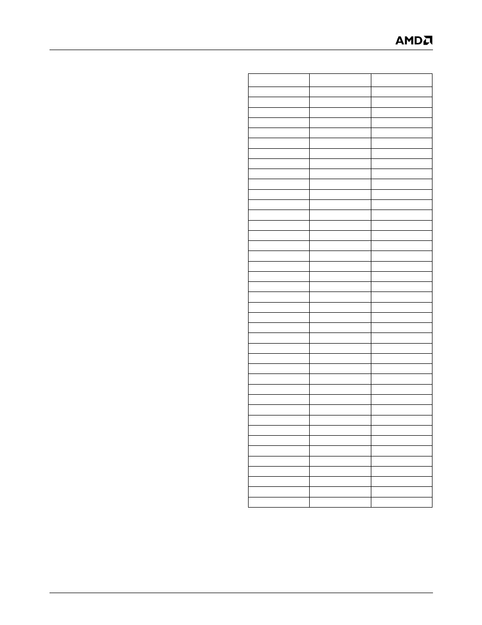
Table 6-3. Cycle Multiplexed PCI / Sub-ISA Balls
PCI
Sub-ISA
Ball No.
AD0
A0
U1
AD1
A1
P3
AD2
A2
U3
AD3
A3
N1
AD4
A4
P1
AD5
A5
N3
AD6
A6
N2
AD7
A7
M2
AD8
A8
M4
AD9
A9
L2
AD10
A10
L3
AD11
A11
K1
AD12
A12
L4
AD13
A13
J1
AD14
A14
K4
AD15
A15
J3
AD16
A16
E1
AD17
A17
F4
AD18
A18
E3
AD19
A19
E2
AD20
A20
D3
AD21
A21
D1
AD22
A22
D2
AD23
A23
B6
AD24
D0
C2
AD25
D1
C4
AD26
D2
C1
AD27
D3
D4
AD28
D4
B4
AD29
D5
B3
AD30
D6
A3
AD31
D7
D5
C/BE0#
D8
L1
C/BE1#
D9
J2
C/BE2#
D10
F3
C/BE3#
D11
H4
PAR
D12
J4
TRDY#
D13
F1
IRDY#
D14
F2
STOP#
D15
G1
DEVSEL#
BHE#
E4