3 crt and tft interface, Figure 9-7, Tft timing diagram – AMD Geode SC2200 User Manual
Page 368: Table 9-19, Tft timing parameters
386
AMD Geode™ SC2200 Processor Data Book
Electrical Specifications
32580B
9.3.3
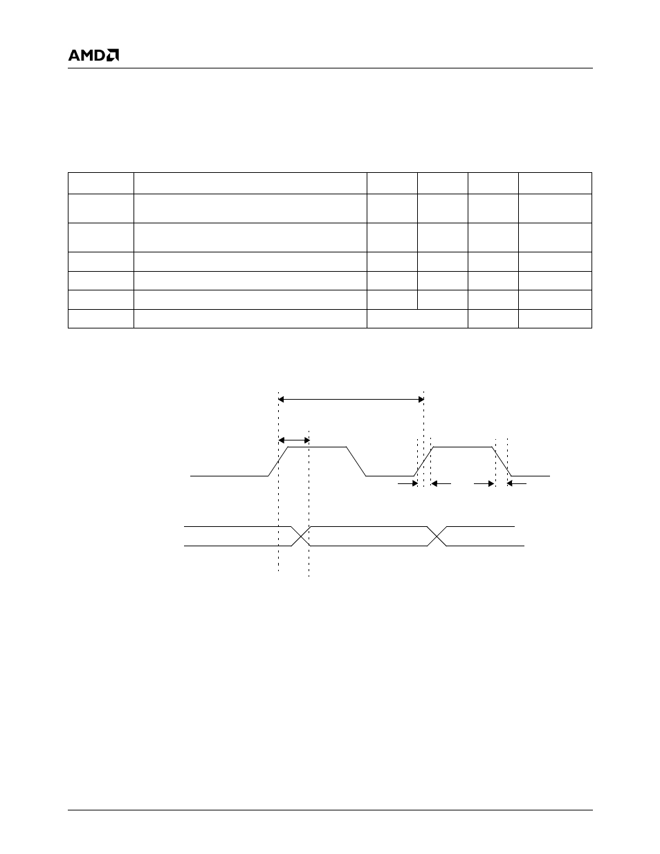
CRT and TFT Interface
Table 9-19 and Figure 9-7 describe the timing of the digital
CRT interface of the SC2200. All measurement points in
this table are identical to the voltage measurement levels
described in Table 9-16 on page 384.
Note that signals DDC_SCL and DDC_SDA of the CRT
interface are compliant with standard ACCESS.bus timing
and are controlled by software.
Figure 9-7. TFT Timing Diagram
Table 9-14. TFT Timing Parameters
Symbol
Parameter
Min
Max
Unit
Comments
t
OV
TFTD[17:0], TFTDE valid time after TFTDCK rising
edge (multiplexed on IDE)
0
8
ns
t
OV
TFTD[17:0], TFTDE valid time after TFTDCK rising
edge (multiplexed on Parallel Port)
0
4
ns
t
CLK_RF
TFTDCK rise/fall time between 0.8V and 2.0V
3
ns
Note 1
t
CLK_P
TFTDCK period time (multiplexed on IDE)
25
ns
t
CLK_P
TFTDCK period time (muxed on Parallel Port)
12.5
ns
t
CLK_D
TFTDCK duty cycle
40/60
%
Note 1. Guaranteed by characterization
t
OV
t
CLK_RF
t
CLK_P
TFTDCK
TFTD[17:0]
TFTDE