1 video input port (vip), 1 direct video mode, Figure 7-4 – AMD Geode SC2200 User Manual
Page 311: Vip block diagram
AMD Geode™ SC2200 Processor Data Book
323
Video Processor Module
32580B
7.2.1
Video Input Port
(VIP)
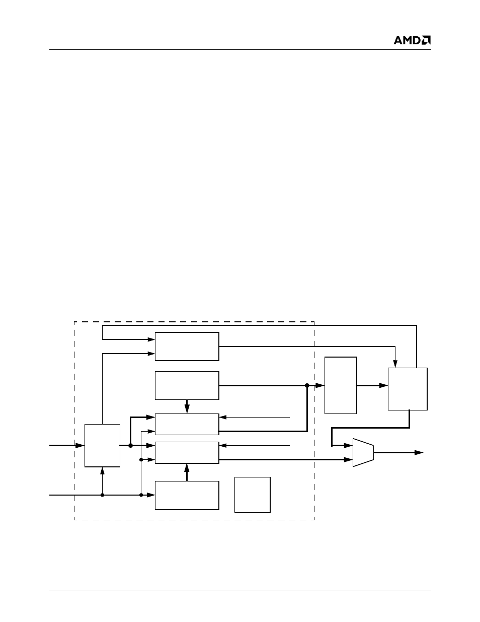
The VIP block is designed to interface the SC2200 with
external video processors (e.g., Philips PNX1300 or Sigma
Designs EM8400) or external TV decoders (e.g., Philips
SAA7114). It inputs CCIR-656 Video and raw VBI data
sourced by those devices, decodes the data, and delivers
the data directly to the Video Formatter (Direct Video
mode) or to the GX1 module’s video frame buffer (Capture
Video/VBI modes). Figure 7-4
shows a diagram of the VIP
block.
From the VIP block’s perspective, Direct Video mode is
always on. There are no registers that enable/disable
Direct Video mode. The data source selected at the video
mux (F4BAR0+Memory Offset 400h[1:0]) determines if the
data from the VIP interface is moved directly or must be
captured.
Two FIFOs in the VIP block support the efficient movement
of Video and VBI data. For Capture Video/VBI modes, a
128-byte FIFO buffers both Video and raw VBI data pro-
cessed by the CCIR-656 decoder. For Direct Video mode,
there is a 2048-byte FIFO that buffer the CCIR-656
decoder’s video data. The FIFOs are also used to provide
clock domain changes. The VIP interface clock (nominally
27 MHz) is the input clock domain for both FIFOs. For the
Capture Video/VBI FIFO, the data is clocked out using the
FPCI clock (33 or 66 MHz). For the Direct Video
FIFO, the
Video data is clocked out using the GX1’s Video port clock
(75, 116, or 133 MHz GX1 core clock divided by 2 or 4).
7.2.1.1
Direct Video Mode
As stated previously, Direct Video mode is on by default so
no registers need to be programmed to support this mode
other than to select the direct video data at the video mux.
The video mux control register is located at
F4BAR0+Memory Offset 400h[1:0].
Direct Video mode while supported is not an optimal mode
of operation. The vertical sync signal is affected by this
mode which cause some CRT monitors operate incorrectly.
This mode supports only one vertical resolution and refresh
rate, which is that of the incoming data. Horizontal resolu-
tion can be scaled if desired. Since the incoming data has
odd and even fields, incoming line must be doubled for it to
display properly. This is equivalent to the Bob technique
which is explained later in this section.
GenLock
Because video input data from the VIP is sent directly,
without significant buffering frame-to-field synchronization
is required with the GX1 module’s graphics data. This syn-
chronization is known as GenLock. The GenLock registers
are located at F4BAR0+Memory Offset 420h and 424h.
Figure 7-4. VIP Block Diagram
CCIR-656
Decoder
Capture Video/VBI
Direct Video
Capture Video/VBI
Controller and
Capture Video/VBI Data
Fast-PCI Clock
Bus Master
FIFO
FIFO
Fast
X-Bus
to
Fast-PCI
Bridge
GX1
Module
Fast-PCI
Direct Video/VBI
Controller
VIP
Data
VIP
Clock
GX1 Video Clock
Direct Video Data
F4BAR2
Control
Registers
Video
Mux
to Video
Formatter
Video or VBI Data
GenLock
Control
Stop DCLK
CRT_VSYNC
VIP_VSYNC
VIP