AMD Geode SC2200 User Manual
Page 282
294
AMD Geode™ SC2200 Processor Data Book
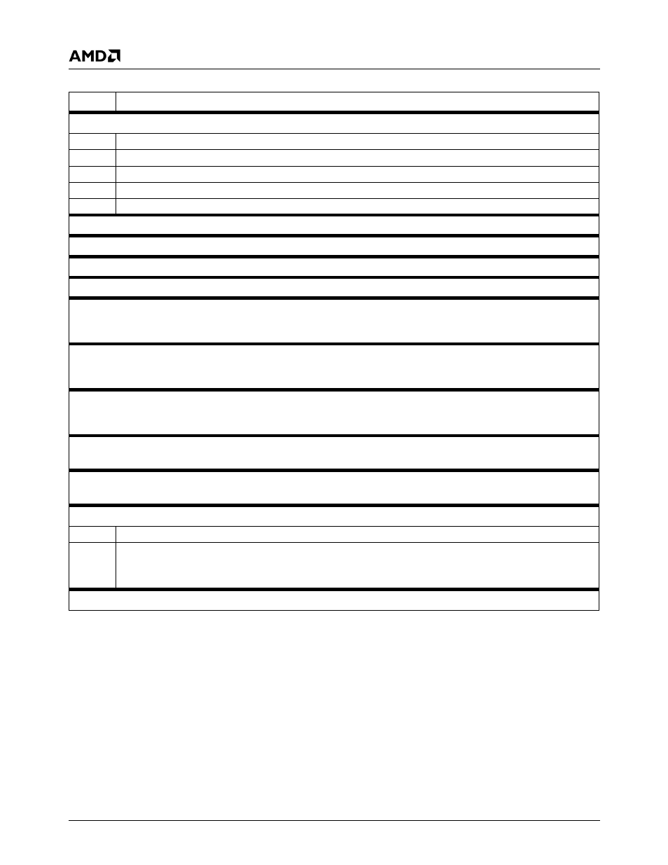
Core Logic Module - USB Controller Registers - PCIUSB
32580B
Index 10h-13h
Base Address Register- USB_BAR0 (R/W)
Reset Value: 00000000h
31:12
Base Address. POST writes the value of the memory base address to this register.
11:4
Always 0. Indicates that a 4 KB address range is requested.
3
Always 0. Indicates that there is no support for prefetchable memory.
2:1
Always 0. Indicates that the base register is 32-bits wide and can be placed anywhere in 32-bit memory space.
0
Always 0. Indicates that the operational registers are mapped into memory space.
Index 14h-2Bh
Reserved
Reset Value: 00h
Index 2Ch-2Dh
Subsystem Vendor ID (RO)
Reset Value: 0E11h
Index 2Eh-2Fh
Subsystem ID (RO)
Reset Value: A0F8h
Index 30h-3Bh
Reserved
Reset Value: 00h
Index 3Ch
Interrupt Line Register (R/W)
Reset Value: 00h
This register identifies the system interrupt controllers to which the device’s interrupt pin is connected. The value of this register is used
by device drivers and has no direct meaning to USB.
Index 3Dh
Interrupt Pin Register (R/W)
Reset Value: 01h
This register selects which interrupt pin the device uses. USB uses INTA# after reset. INTB#, INTC# or INTD# can be selected by writ-
ing 2, 3 or 4, respectively.
Index 3Eh
Min. Grant Register (RO)
Reset Value: 00h
This register specifies how long a burst is needed by the USB, assuming a clock rate of 33 MHz. The value in this register specifies a
period of time in units of 1/4 microsecond.
Index 3Fh
Max. Latency Register (RO)
Reset Value: 50h
This register specifies how often (in units of 1/4 microsecond) the USB needs access to the PCI bus assuming a clock rate of 33 MHz.
Index 40h-43h
ASIC Test Mode Enable Register (R/W)
Reset Value: 000F0000h
Used for internal debug and test purposes only.
Index 44h
ASIC Operational Mode Enable Register (R/W)
Reset Value: 00h
7:1
Write Only. Read as 0s.
0
Data Buffer Region 16
0: The size of the region for the data buffer is 32 bytes.
1: The size of the region for the data buffer is 16 bytes.
Index 45h-FFh
Reserved
Reset Value: 00h
Table 6-41. PCIUSB: USB PCI Configuration Registers (Continued)
Bit
Description