Figure 9-8, Figure 9-9, Acb start and stop condition timing diagram – AMD Geode SC2200 User Manual
Page 371: Ition, note 2, Note 2
AMD Geode™ SC2200 Processor Data Book
389
Electrical Specifications
32580B
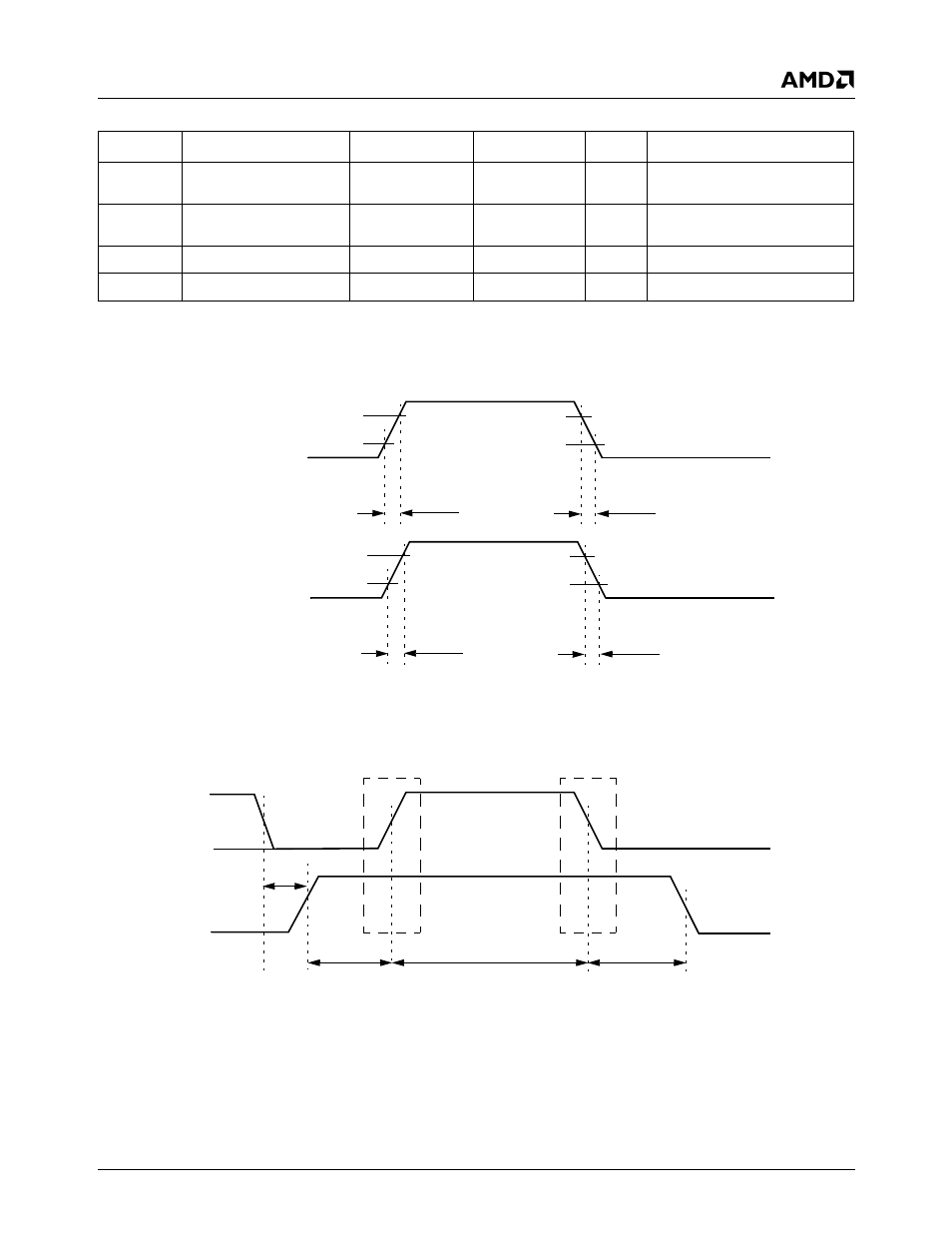
Figure 9-8. ACB Signals: Rising Time and Falling Timing Diagram
Figure 9-9. ACB Start and Stop Condition Timing Diagram
t
SDAfo
AB1D/AB2D signal fall
time
300 ns
t
SDAro
AB1D/AB2D signal rise
time
1
μs
t
SDAho
AB1D/AB2D hold time
7
*
t
CLK
- t
SCLfo
After AB1C/AB2C falling edge
t
SDAvo
AB1D/AB2D valid time
7
*
t
CLK
+ t
RD
After AB1C/AB2C falling edge
Note 1. K is determined by bits [7:1] of the ACBCTL2 register (LDN 05h/06h, Offset 05h).
Note 2. t
SCLhigho
value depends on the signal capacitance and the pull-up value of the relevant pin.
Table 9-17. ACCESS.bus Output Timing Parameters (Continued)
Symbol
Parameter
Min
Max
Unit
Comments
AB1D
t
SDAr
0.7V
IO
0.3V
IO
t
SDAf
0.7V
IO
0.3V
IO
AB1C
t
SCLr
0.7V
IO
0.3V
IO
t
SCLf
0.7V
IO
0.3V
IO
AB2D
AB2C
AB1D
AB1C
t
CSTOsi
t
BUFi
t
DLCs
t
CSTRhi
Start Condition
Stop Condition
t
DLCo
t
CSTOso
t
BUFo
t
CSTRho
AB2D
AB2C
- Radeon 4850 (18 pages)
- Phenom AM2r2 (6 pages)
- GA-K8N51GMF-9 (80 pages)
- Socket AM2+ Quad Core Processor SB750 (63 pages)
- Turion 64 X2 (2 pages)
- GA-M61PM-S2 (80 pages)
- Socket AM2+ Quad Core AMD Processor 790GX (53 pages)
- 7ZMMC (36 pages)
- Geode SC1200 (443 pages)
- CS5535 (36 pages)
- Geode LX800 (46 pages)
- ATI RADEON HD 2600 (62 pages)
- LE-363 (45 pages)
- SimNow Simulator 4.4.4 (269 pages)
- GA-MA69VM-S2 (88 pages)
- KM780V (21 pages)
- SBX-5363 (55 pages)
- AM79C971 (1 page)
- K3780E-S (43 pages)
- GEODE LE-366 (45 pages)
- 7ZX-1 (46 pages)
- Phenom II (6 pages)
- ATI Radeon x1700 FSC (22 pages)
- Turion 64 (3 pages)
- 1207 (62 pages)
- CrossFire 550X (16 pages)
- Athlon 27488 (104 pages)
- Geode LX [email protected] (680 pages)
- GA-M61SME-S2 (80 pages)
- N2PA-LITE (45 pages)
- GA-K8NSC-939 (80 pages)
- GEODE NX800LX (27 pages)
- Am79C930 (161 pages)
- LV-651 (50 pages)
- Athlon 6 (19 pages)
- Geode SC3200 (428 pages)
- SEMPRON 10 (102 pages)
- GA-K8N ULTRA-9 (80 pages)
- Geode LX CS5536 (8 pages)
- MINI-ITX LV-651 (50 pages)
- GA-K8N51GMF-RH (88 pages)
- ATI RADEON HD 2400 (64 pages)
- GA-M55S-S3 (88 pages)
- GA-M51GM-S2G (88 pages)