21 udc endpoint x data register (uddr5/10/15), 7 usb device controller register summary, 21 udc endpoint x data register (uddr5/10/15) -48 – Intel PXA255 User Manual
Page 450: 7 usb device controller register summary -48, Table 12-31
12-48
Intel® PXA255 Processor Developer’s Manual
USB Device Controller
12.6.21
UDC Endpoint x Data Register (UDDR5/10/15)
UDDR5/10/15, shown in
, is an interrupt IN endpoint that is 8 bytes deep. Data must be
loaded via direct Megacell writes. Because the USB system is a host initiator model, the host must
poll Endpoint 5 to determine interrupt conditions. The UDC can not initiate the transaction.
12.7
USB Device Controller Register Summary
shows the registers associated with the UDC and the physical addresses used to access
them.
Table 12-31. UDDR4/9/14 Bit Definitions
0x 4060_0400
0x 4060_0900
0x 4060_0E00
UDDR4
UDDR9
UDDR14
USB Device Controller
Bit
31 30 29 28 27 26 25 24 23 22 21 20 19 18 17 16 15 14 13 12 11 10 9
8
7
6
5
4
3
2
1
0
reserved
8-bit Data
Reset x
x
x
x
x
x
x
x
x
x
x
x
x
x
x
x
x
x
x
x
x
x
x
x
0
0
0
0
0
0
0
0
Bits
Name
Description
31:8
—
reserved
7:0
DATA
Top of endpoint data currently being loaded
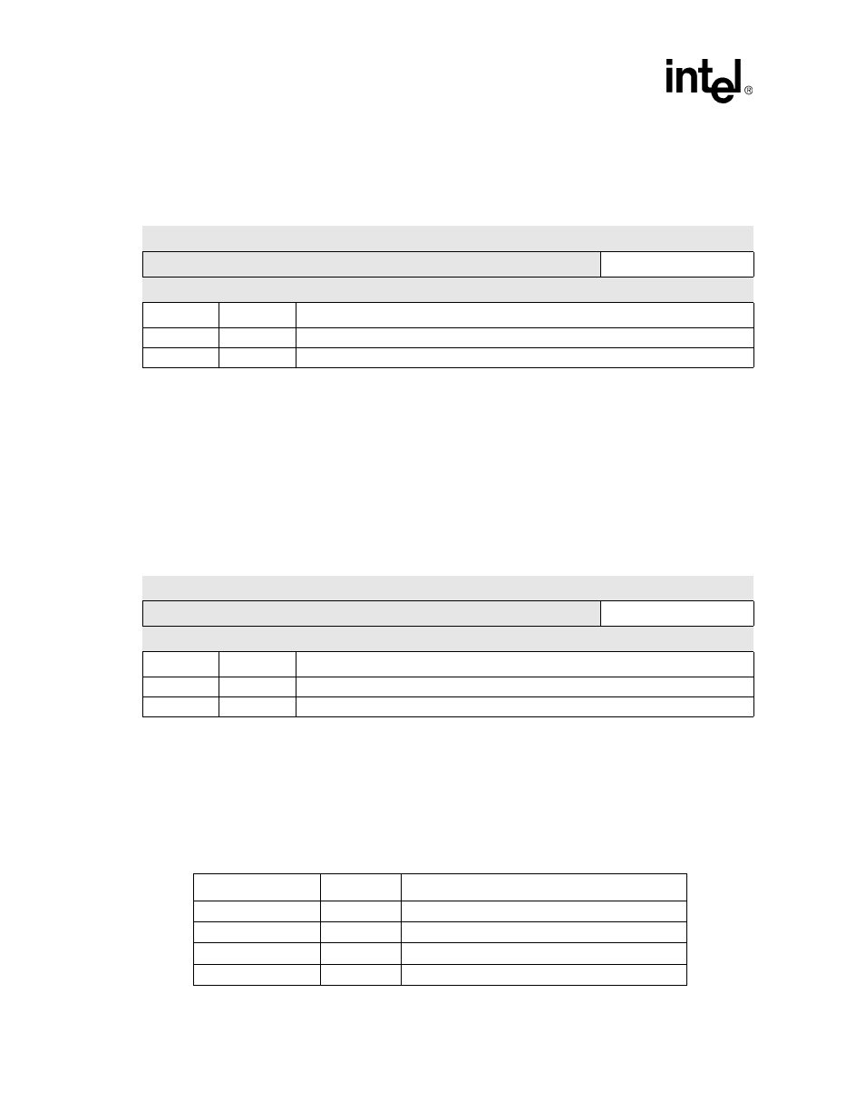
Table 12-32. UDDR5/10/15 Bit Definitions
0x 4060_00A0
0x 4060_00C0
0x 4060_00E0
UDDR5
UDDR10
UDDR15
USB Device Controller
Bit
31 30 29 28 27 26 25 24 23 22 21 20 19 18 17 16 15 14 13 12 11 10 9
8
7
6
5
4
3
2
1
0
reserved
8-bit Data
Reset x
x
x
x
x
x
x
x
x
x
x
x
x
x
x
x
x
x
x
x
x
x
x
x
0
0
0
0
0
0
0
0
Bits
Name
Description
31:8
—
reserved
7:0
DATA
Top of endpoint data currently being loaded
Table 12-33. USB Device Controller Register Summary (Sheet 1 of 3)
Address
Name
Description
0x4060_0000
UDCCR
UDC Control Register
0x4060_0004
—
reserved for future use
0x4060_0008
UDCCFR
UDC Control Function Register
0x4060_000C
—
reserved for future use