1 receive fifo interrupt enable (rie), 2 transmit fifo interrupt enable (tie), 3 loop back mode (lbm) – Intel PXA255 User Manual
Page 322

8-12
Intel® PXA255 Processor Developer’s Manual
Synchronous Serial Port Controller
8.7.2.1
Receive FIFO Interrupt Enable (RIE)
The Receive FIFO Interrupt Enable (RIE) bit is used to mask or enable the receive FIFO service
request interrupt. When RIE=0, the interrupt is masked and the interrupt controller ignores the state
of the Receive FIFO Service Request (RFS) bit in the SSPC Status Register. When the RIE bit is
set to a 1, the interrupt is enabled and, if the RFS bit is set to a 1, an interrupt request is made to the
interrupt controller. If the RIE bit is set to 0 neither the RFS bit’s current state nor the receive FIFO
logic’s ability to set and clear the RFS bit is affected. However, the interrupt request generation is
blocked.
The RIE bit’s state does not affect the receive FIFO DMA request generation that is asserted when
the RFS bit is set to a 1.
8.7.2.2
Transmit FIFO Interrupt Enable (TIE)
The Transmit FIFO Interrupt Enable (TIE) bit is used to mask or enable the transmit FIFO service
request interrupt. When the TIE bit is set to a 0, the interrupt is masked and the interrupt controller
ignores the state of the Transmit FIFO Service Request (TFS) bit in the SSPC Status Register.
When the TIE bit is set to a 1, the interrupt is enabled and, if the TFS bit is set to a 1, an interrupt
request is made to the interrupt controller. If the TIE bit is set to a 0, neither the TFS bit’s current
state nor the transmit FIFO logic’s ability to set and clear the TFS bit is affected. However, the
interrupt request generation is blocked.
The TIE bit’s state does not affect the transmit FIFO DMA request generation that is asserted when
the TFS bit is set to a 1.
8.7.2.3
Loop Back Mode (LBM)
The loop back mode (LBM) bit is used to enable and disable the SSP transmit and receive logic.
When LBM=0, the SSP operates normally. The transmit and receive data paths are separate and
communicate via their respective pins. However, since the SSP is a master device, it must transmit
in order to receive while in either SSP or SPI mode. When LBM=1, the transmit serial shifter’s
output is directly connected internally to the receive serial shifter’s input.
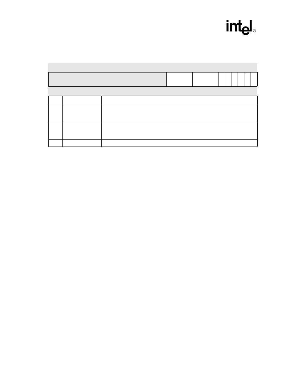
9:6
TFT
(Transmit FIFO
Threshold)
Sets threshold level at which Transmit FIFO generates an interrupt or DMA request. This
level must be set to the desired threshold value minus 1.
13:10
RFT
(Receive FIFO
Threshold)
Sets threshold level at which Receive FIFO generates an interrupt or DMA request. This
level must be set to the desired threshold value minus 1.
31:14
—
reserved
Table 8-3. SSCR1 Bit Definitions (Sheet 2 of 2)
0x4100_0004
SSP Control Register 1 (SSCR1)
Synchronous Serial Port Controller
Bit
31 30 29 28 27 26 25 24 23 22 21 20 19 18 17 16 15 14 13 12 11 10 9
8
7
6
5
4
3
2
1
0
reserved
RFT
TFT
MW
D
S
SP
H
SPO
LB
M
TIE
RI
E
Reset
X
0x0
0x0
0
0
0
0
0
0
Bits
Name
Description
