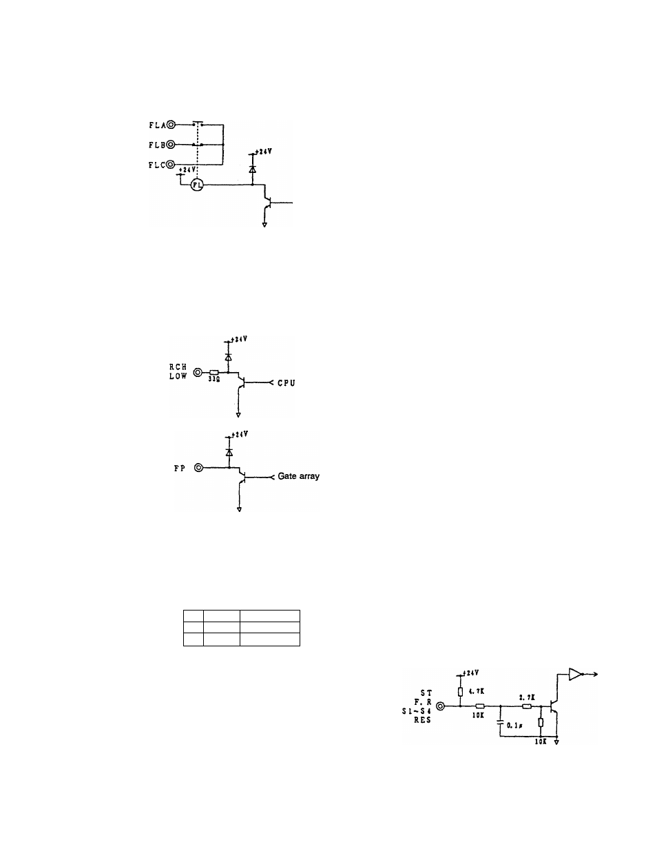
Internal circuit diagram, T. la t, Iy©b – Toshiba Tosvert VF-A5 User Manual
Page 28
Attention! The text in this document has been recognized automatically. To view the original document, you can use the "Original mode".

Fig. 6.2.1 Input/output internal circuits (2/2)
Sym
bol
Internal circuit diagram
Sym
bol
internal circuit diagram
e
©
©
(D
Ф
< CPU
_a»v
_
t. la T
P2 < ®----------
------- *
Fuse resistor
Analog output
4.7k
cc ©—
0. u
= T
-< CPU
Low-pass
filter
circuit
Response
Resolution
AM
3mS
1/256
PM
lOOmS
1/1024 or better
PP ®-
OOQ
5. l V x 2
■jü. lA
CC ©------1
©
о
©
Analog input
(0~10Vdo)
18k
-o-
+ 5V
2^
RR ©-
Note 1) Ф
CC ®------
l l 5 k
2 Í
0. 1
a
A/D converter
SVmax
Analog input
O-'IOVdc, 0~20mAdc)
IY©b
Note 1)
CC ©------
18k
-cu-
+ 5V
2^
h o o s
5k 2i
A/D converter
SVmax
Cb-IOVdo (switch at V side)
4~20mAdc (swKch at I side)
-F/-Analog input
+
5
V
(o~+/-iovac. (K+/-5Yac)
Voltage converter clrcuft^ ^
RX <§>—
Note 1)
Ik 33k 33k
------ CD- -Oj-CD—
CC @—
0
.
i M
A/D converter
2.5V±2.5V
0~6Vdc (switch at 5 side)
0—10Vdc (switch at 10 side)
CC
@-
C/l@-
j.
Grounding
capacitor
22piF
Contact inputs
CPU
Note 1) A capacitor is installed on the analog input terminals (RR, RX, IV), so if an output such as an
operational amplifier is directly connected to these terminals, instability may result. Always pass signals
of this type to these terminals through a lOOft to Ikfi resistor.
-22
