24 master frequency input (dfin), Master frequency input (dfin), Function library – Lenze EVS9332xS User Manual
Page 114: Function blocks
Function library
Function blocks
3.2.24
Master frequency input (DFIN)
3−62
l
EDSVS9332S−EXT EN 2.0
3.2.24
Master frequency input (DFIN)
Purpose
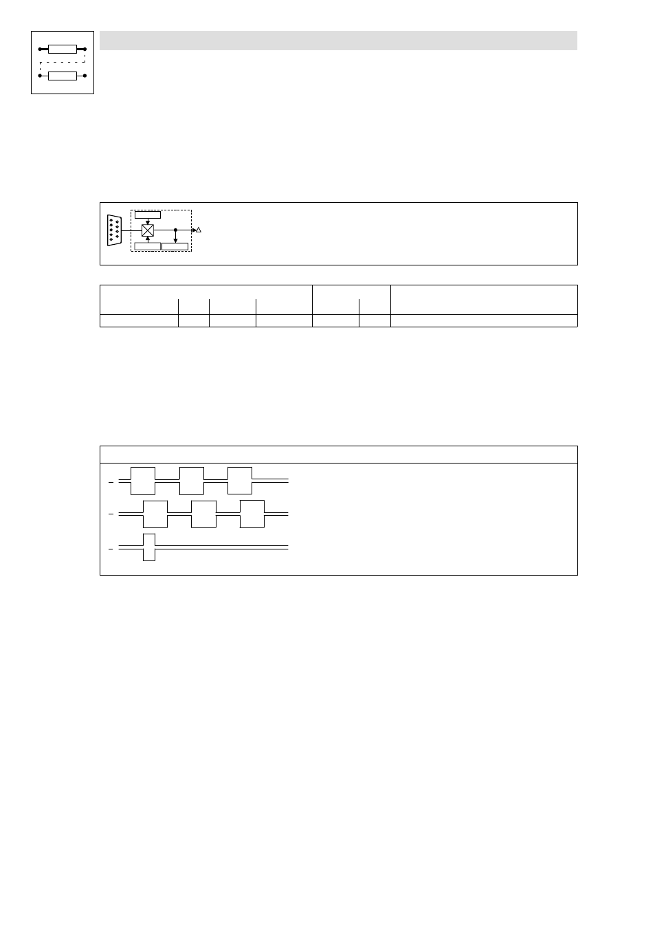
Converting and scaling a power pulse current at the digital frequency input X9 into a speed and phase
setpoint. The digital frequency is transferred in a high−precision mode (with offset and gain errors).
C0425
DFIN
DFIN-OUT
C0426
X9
C0427
Fig. 3−58
Digital frequency input (DFIN)
Signal
Source
Note
Name
Type
DIS
DIS format
CFG
List
DFIN−OUT
phd
C0426
dec [rpm]
−
−
Function
l
The input X9 is designed for signals with TTL level.
l
In the event of digital frequency cascade or digital frequency rail, adapt the drive to the
connected encoder or controller via C0425.
l
The input of a zero track is optional.
l
Via C0427 the following input signals can be evaluated:
C0427 = 0
O
O
B
B
Z
Z
Fig. 3−59
Phase−delayed signal sequence (CW rotation)
CW rotation
Track A is leading track B by 90 (positive value at DFIN−OUT).
CCW rotation
Track A is lagging track B by 90 (negative value at DFIN−OUT).