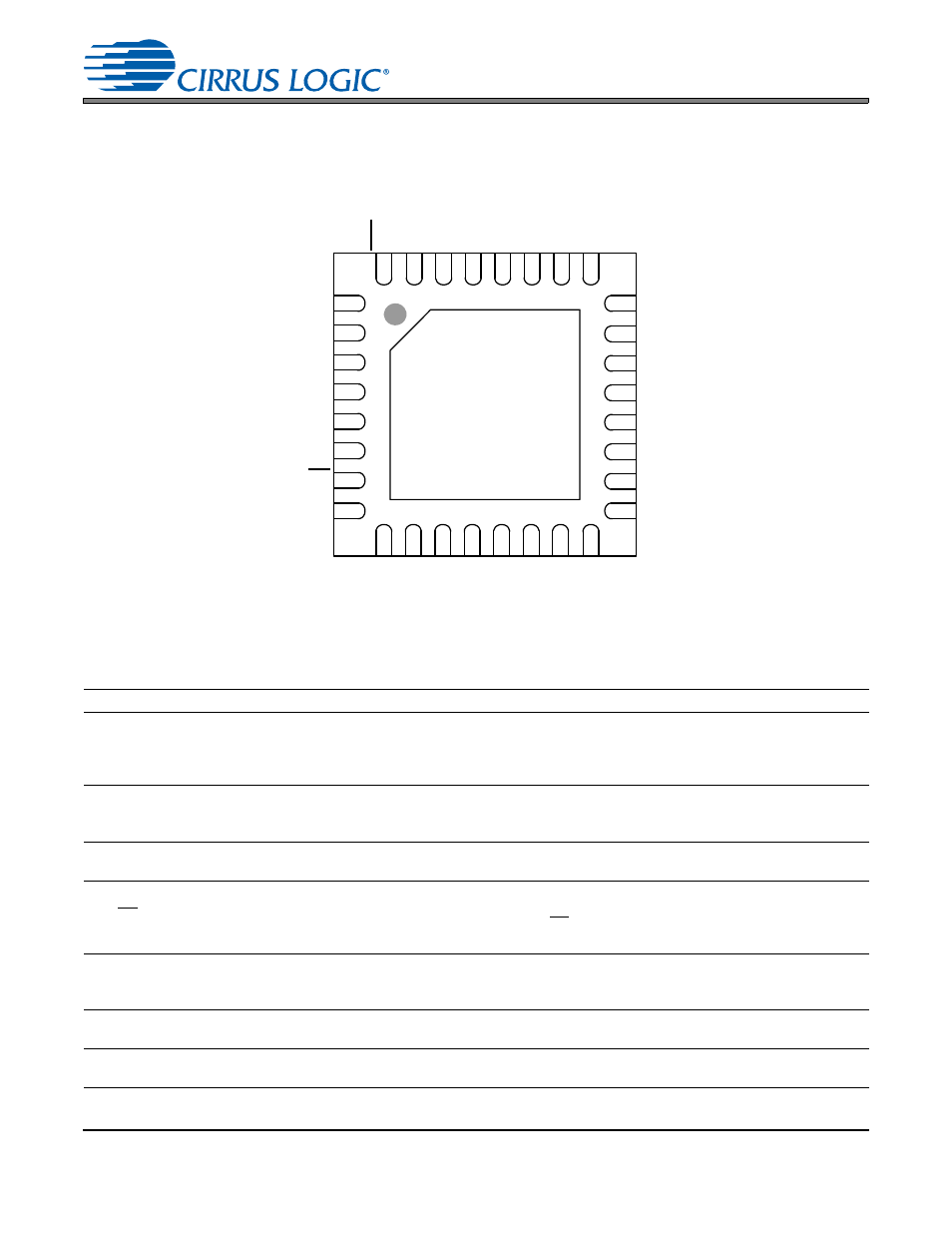
Pin description, 1 software mode – Cirrus Logic CS8422 User Manual
Page 9

DS692F2
9
CS8422
1. PIN DESCRIPTION
1.1
Software Mode
Pin Name
Pin #
Pin Description
RX[3:0],
RXP/RXN[1:0]
1
2
5
6
AES3/SPDIF Input (Input) - Single-ended or differential receiver inputs carrying AES3 or S/PDIF
encoded digital data. RX[3:0] comprise the single-ended input multiplexer. RXP[1:0] comprise the
non-inverting inputs of the differential input multiplexer and RXN[1:0] comprise the inverting inputs
of the differential input multiplexer. Unused inputs should be tied to AGND/DGND.
VA
3
Analog Power (Input) - Analog power supply, nominally +3.3 V. Care should be taken to ensure
that this supply is as noise-free as possible, as noise on this pin will directly affect the jitter perfor-
mance of the recovered clock.
AGND
4
Analog Ground (Input) - Ground for the analog circuitry in the chip. AGND and DGND should be
connected to a common ground area under the chip.
AD0/CS
7
Address Bit 0 (I²C) / Software Chip Select (SPI) (Input) - A falling edge on this pin puts the
CS8422 into SPI Control Port Mode. With no falling edge, the CS8422 defaults to I²C Mode. In I²C
Mode, AD0 is a chip address pin. In SPI Mode, CS is used to enable the control port interface on
the CS8422. See
“Control Port Description” on page 43
.
AD1/CDIN
8
Address Bit 1 (I²C) / Serial Control Data in (SPI) (Input) - In I²C Mode, AD1 is a chip address pin.
In SPI Mode, CDIN is the input data line to the control port interface. See
SCL/CCLK
9
Software Clock (Input) - Serial control interface clock used to clock control data bits into and out of
the CS8422.
SDA/CDOUT
10
Serial Control Data I/O (I²C) / Data Out (SPI) (Input/Output) - In I²C Mode, SDA is the control I/O
data line. In SPI Mode, CDOUT is the output data from the control port interface on the CS8422.
10
9
8
7
6
5
4
3
2
1
11
12
13
14
15
16
17
18
19
20
21
22
23
24
25
26
27
28
29
30
31
32
Top-Down View
32-Pin QFN Package
Thermal Pad
XTO
IL
RCK
GPO
3
OLRCK1
OSC
L
K
1
SDOUT1
OSCLK2
VA
AGND
AD0/CS
RX0/RXP0
SDOUT2
VL
TDM
_
IN
OLR
CK2
RX1/RXN0
RX2/RXP1
RX3/RXN1
RMCK
GPO2
VD_FILT
V_REG
XTI
AD1/CDIN
SD
A/CD
OU
T
SC
L/CCLK
ISCLK
GPO1
GPO0
SDIN
DGND
RST
