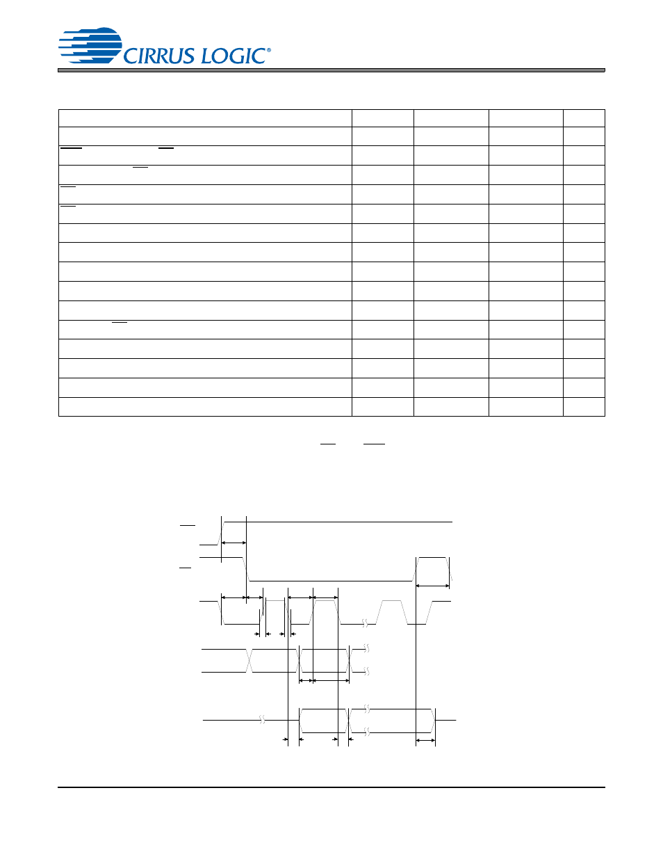
Figure 5.spi mode timing – Cirrus Logic CS8422 User Manual
Page 20
20
DS692F2
CS8422
SWITCHING CHARACTERISTICS - CONTROL PORT - SPI MODE
Inputs: Logic 0 = 0 V, Logic 1 = VL; C
L
= 20 pF.
Notes:
13. t
spi
only needed before first falling edge of CS after RST rising edge. t
spi
= 0 at all other times.
14. Data must be held for sufficient time to bridge the transition time of CCLK.
15. CDOUT should not be sampled during this time.
16. For f
sck
< 1 MHz.
Parameter
Symbol
Min
Max
Unit
CCLK Clock Frequency
f
sck
0
6.0
MHz
RST Rising Edge to CS Falling
t
srs
500
-
µs
CCLK Edge to CS Falling
t
spi
500
-
ns
CS High Time Between Transmissions
t
csh
1.0
-
µs
CS Falling to CCLK Edge
t
css
20
-
ns
CCLK Low Time
t
scl
66
-
ns
CCLK High Time
t
sch
66
-
ns
CDIN to CCLK Rising Setup Time
t
dsu
40
-
ns
CCLK Rising to DATA Hold Time
t
dh
15
-
ns
CCLK Falling to CDOUT Valid
t
scdov
-
100
ns
Time from CS Rising to CDOUT High-Z
t
cscdo
-
100
ns
CDOUT Rise Time
t
r1
-
25
ns
CDOUT Fall Time
t
f1
-
25
ns
CCLK and CDIN Rise Time
t
r2
-
100
ns
CCLK and CDIN Fall Time
t
f2
-
100
ns
t r2
t f2
t dsu tdh
t sch
t scl
CS
CCLK
CDIN
tcss
t csh
t spi
t srs
RST
CDOUT
t scdov
t scdov
t cscdo
Hi-Impedance
Figure 5. SPI Mode Timing