3 recovered master clock - rmck, 1 hardware mode control, 2 software mode control – Cirrus Logic CS8422 User Manual
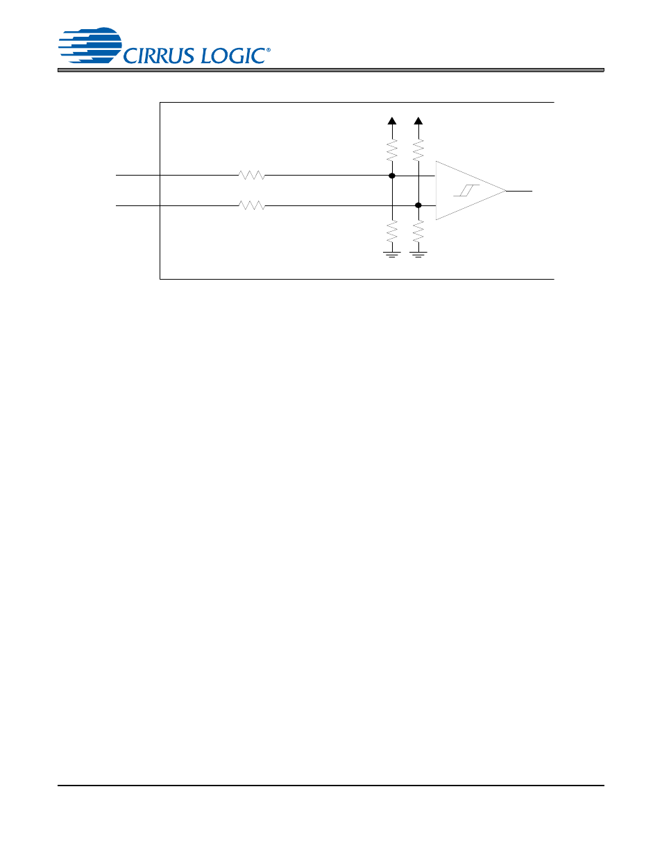
Page 31: 4 xti system clock mode, Figure 18.differential receiver input structure, Figure 18, Cs8422

DS692F2
31
CS8422
Figure 18. Differential Receiver Input Structure
6.3
Recovered Master Clock - RMCK
The CS8422 has an internal PLL which recovers a high-frequency system clock, referred to as the recov-
ered master clock (RMCK). RMCK can be generated by incoming AES3-compatible data or the ISCLK
(slave mode and Software Mode only). This clock is used as the master clock source for the AES3 receiver
and the master-mode serial port that it directly supplies data to, and is available as an output on the RMCK
pin. In addition, the user can set the RMCK as the master clock of either of the two remaining serial ports.
6.3.1
Hardware Mode Control
In Hardware Mode, the RMCK frequency is determined by the incoming AES3 frame rate and the
MS_SEL pin. RMCK can be routed for use as the master clock for the serial audio output associated with
SDOUT1 by connecting a 20 k
resistor from the RMCK pin to VL. See
for more details.
6.3.2
Software Mode Control
In Software Mode, The RMCK frequency is determined by the incoming AES3 frame rate or ISCLK/64
(slave mode only). The RMCK frequency is configured in the register described in
ered Master Clock Ratio Control & Misc. (09h)” on page 53
. If the ISCLK is chosen as the source for RM-
CK, then the ratios in the
“Recovered Master Clock Ratio Control & Misc. (09h)”
register reflect the ratio
of 64*RMCK/ISCLK.
6.4
XTI System Clock Mode
A special clock switching mode is available that allows the clock present at the XTI-XTO clock input to au-
tomatically replace RMCK when the PLL becomes unlocked. This is accomplished without spurious transi-
tions or glitches on RMCK.
When clock switching is enabled, the PLL’s loss of lock will cause the XTI-XTO clock input to be output on
RMCK. If a serial port is set master mode and has RMCK as its master clock source, its LRCK and SCLK
+
-
V A
(2 2 0 0 0 /N )
A G N D
R X P [1 :0 ]
(1 5 0 0 + 1 5 0 0 /N )
(2 2 0 0 0 /N )
R X N [1 :0 ]
(1 5 0 0 + 1 5 0 0 /N )
(2 2 0 0 0 /N )
(2 2 0 0 0 /N )
Note:
1.
If RXP/N[1:0] is selected by either the receiver MUX or the TX pass-through MUX, N=1.
2.
If RXP/N[1:0] is selected by both the receiver MUX and the TX pass-through MUX, N=2.
3.
If RXP/N[1:0] is not selected at all, N=0 (i.e. high impedance).
