2 i·c mode, 3 memory address pointer (map), 2 i²c mode 9.1.3 memory address pointer (map) – Cirrus Logic CS8422 User Manual
Page 44: Cs8422, 2 i²c mode
44
DS692F2
CS8422
9.1.2
I²C Mode
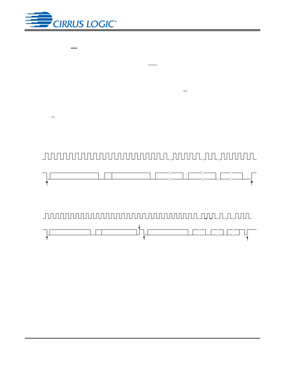
In I²C Mode, SDA is a bidirectional data line. Data is clocked into and out of the part by the clock, SCL.
There is no CS pin. Pins AD0 and AD1 form the two least significant bits of the chip address and should
be connected to VL or DGND as desired. The GPO2 pin is used to set the AD2 bit by connecting a 20 k
resistor from the GPO2 pin to VL (a 20 k
pull-up sets AD2 = 1, and the absence of a pull-up sets
AD2 = 0). The states of the pins are sensed after RST is released.
The signal timings for a read and write cycle are shown in
and
. A Start condition is
defined as a falling transition of SDA while the clock is high. A Stop condition is a rising transition while
the clock is high. All other transitions of SDA occur while the clock is low. The first byte sent to the CS8422
after a Start condition consists of a 7-bit chip address field and a R/W bit (high for a read, low for a write).
The upper 4 bits of the 7-bit address field are fixed at 0010.
To communicate with a CS8422, the chip address field, which is the first byte sent to the CS8422, should
match 0010 followed by the settings of the AD2, AD1, and AD0 pins. The eighth bit of the address is the
R/W bit. If the operation is a write, the next byte includes the Memory Address Pointer (MAP) which se-
lects the register to be read or written. If the operation is a read, the contents of the register pointed to by
the MAP will be output. Each byte is separated by an acknowledge bit (ACK). The ACK bit is output from
the CS8422 after each input byte is read, and is input to the CS8422 from the microcontroller after each
transmitted byte.
Note that the read operation can not set the MAP so an aborted write operation is used as a preamble.
As shown in
, the write operation is aborted after the acknowledge for the MAP byte by sending
a stop condition.
9.1.3
Memory Address Pointer (MAP)
The MAP is an 8-bit word containing the control port address to be read or written in both SPI and I²C Modes
and a bit to control an auto-increment feature. MAP[6:0] constitute the address to be read or written, while
bit 7 of the MAP (INC) determines whether or not MAP[6:0] will automatically increment after each control
port read or write. If INC = 0, MAP[6:0] will not automatically increment after each control port read or write.
If INC = 1, MAP[6:0] will automatically increment after each control port read or write. The MAP byte is
shown in
and
.
4 5 6 7
24 25
SCL
CHIP ADDRESS (WRITE)
MAP BYTE
DATA
DATA +1
START
ACK
STOP
ACK
ACK
ACK
0 0 1 0 AD2 AD1 AD0 0
SDA
6 5 4 3 2 1 0
7 6 1 0
7 6 1 0
7 6 1 0
0 1 2 3
8 9
12
16 17 18 19
10 11
13 14 15
27 28
26
DATA +n
INC
Figure 23. Control Port Timing, I²C Slave Mode Write
SCL
CHIP ADDRESS (WRITE)
MAP BYTE
DATA
DATA +1
START
ACK
STOP
ACK
ACK
ACK
SDA
CHIP ADDRESS (READ)
START
6 5 4 3 2 1 0
7 0
7 0
7 0
NO
16
8 9
12 13 14 15
4 5 6 7
0 1
20 21 22 23 24
26 27 28
2 3
10 11
17 18 19
25
ACK
DATA + n
STOP
0 0 1 0 AD2 AD1 AD0 0
0 0 1 0 AD2 AD1 AD0 1
INC
Figure 24. Control Port Timing, I²C Slave Mode Read