2 hardware mode, Cs8422 – Cirrus Logic CS8422 User Manual
Page 11

DS692F2
11
CS8422
1.2
Hardware Mode
Pin Name
Pin #
Pin Description
RXP/RXN[1:0]
1
2
5
6
AES3/SPDIF Input (Input) - Differential receiver inputs carrying AES3 or S/PDIF encoded digital
data. RXP[1:0] comprise the non-inverting inputs of the differential input multiplexer; and RXN[1:0]
comprise the inverting inputs of the input multiplexer. Unused inputs should be tied to AGND.
VA
3
Analog Power (Input) - Analog power supply, nominally +3.3 V. Care should be taken to ensure that
this supply is as noise-free as possible, as noise on this pin will directly affect the jitter performance of
the recovered clock.
AGND
4
Analog Ground (Input) - Ground for the analog circuitry in the chip. AGND and DGND should be
connected to a common ground area under the chip.
SAOF
7
Serial Audio Output Format Select (Input) - Used to select the serial audio output format after RST
is released. See
for format settings.
MS_SEL
8
Master/Slave Select (Input) - Used to select Master or Slave settings for the output serial audio ports
after RST is released. See
for format settings.
NV/RERR
9
Non-Validity Receiver Error/Receiver Error (Output) - Receiver error indicator. NVERR is output by
default, RERR is selected by a 20 k
resistor to VL.
V/AUDIO
10
Validity Data/AUDIO (Output) - If a 20 k
pull-down is present on this pin, it will output serial Validity
data from the AES3 receiver, clocked by the rising and falling edges of OLRCK2 in master mode. If a
20 k
pull-up is present, the pin will be low when valid linear PCM data is present at the AES3 input.
XTI
11
Crystal/Oscillator In (Input) - Crystal or digital clock input for Master clock. See
.
XTO
12
Crystal Out (Output) - Crystal output for Master clock. See
.
10
9
8
7
6
5
4
3
2
1
11
12
13
14
15
16
17
18
19
20
21
22
23
24
25
26
27
28
29
30
31
32
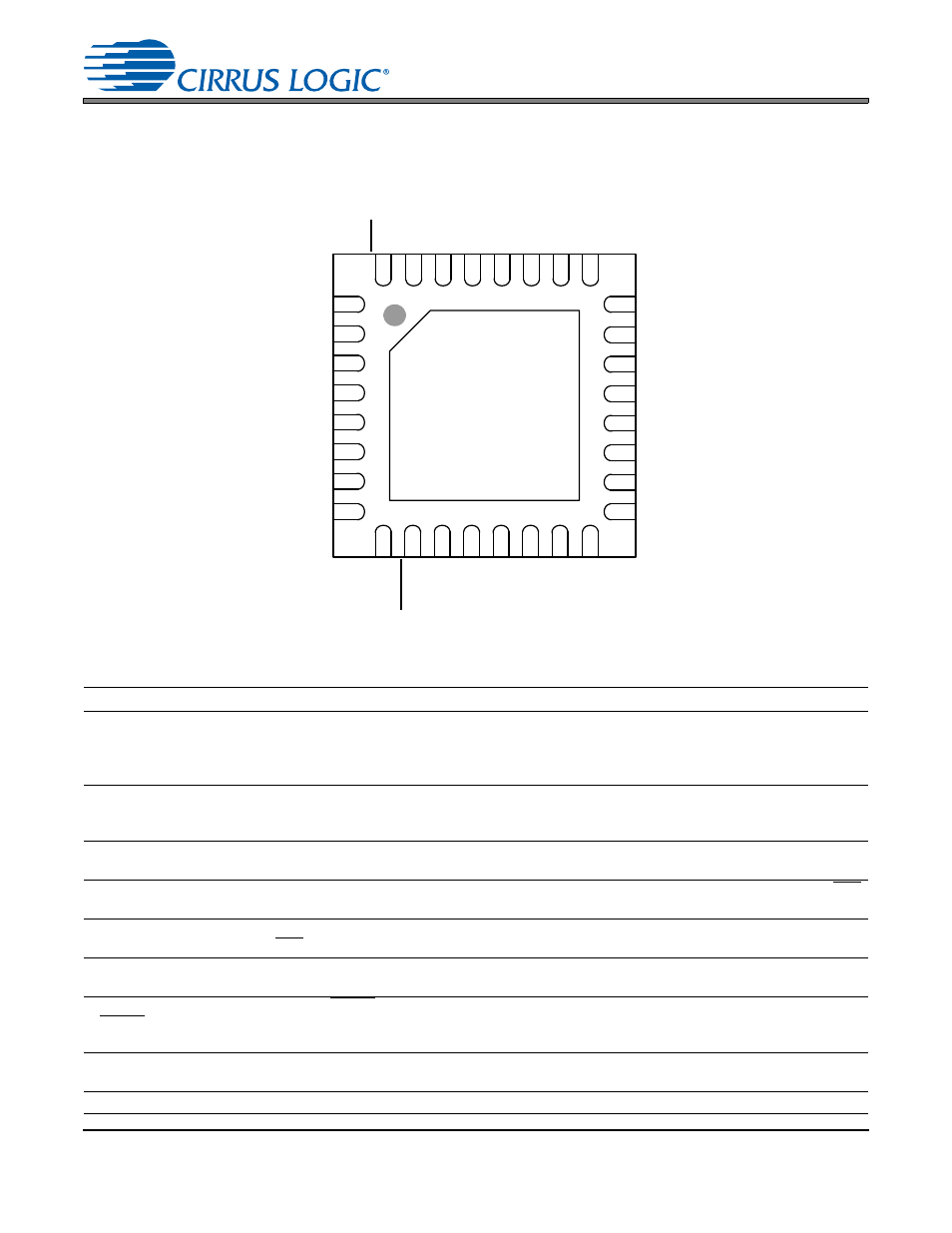
Top-Down View
32-Pin QFN Package
Thermal Pad
XTO
MCLK_
O
UT
S
RC_UNLOCK
SDOUT1
OSCLK2
VA
AGND
SAOF
RXP0
SDOUT2
VL
TDM_
IN
OLRCK
2
RXN0
RXP1
RXN1
RMC
K
TX/U
VD_FILT
V_REG
XTI
MS_SEL
V/AU
DIO
NV
/RER
R
TX_SEL
C
RC
BL
RX_SEL
DGND
RS
T
OSCLK1
OLRCK1
