3 crystal oscillator pins, 4 analog pin summary, Table – Rainbow Electronics AT86RF231 User Manual
Page 6
6
8111A–AVR–05/08
AT86RF231
The RF port DC values depend on the operating state, refer to
Section 7. “Operating Modes” on
In TRX_OFF state, when the analog front-end is disabled (see
), the RF pins are pulled to ground, preventing a floating voltage.
In transmit mode, a control loop provides a common-mode voltage of 0.9V. Transistor M0 is off,
allowing the PA to set the common-mode voltage. The common-mode capacitance at each pin
to ground shall be < 30 pF to ensure the stability of this common-mode feedback loop.
In receive mode, the RF port provides a low-impedance path to ground when transistor M0, see
, pulls the inductor center tap to ground. A DC voltage drop of 20 mV
across the on-chip inductor can be measured at the RF pins.
1.2.3
Crystal Oscillator Pins
XTAL1, XTAL2
The pin XTAL1 is the input of the reference oscillator amplifier (XOSC), XTAL2 is the output. A
detailed description of the crystal oscillator setup and the related XTAL1/XTAL2 pin configura-
tion can be found in
Section 9.6 “Crystal Oscillator (XOSC)” on page 116
When using an external clock reference signal, XTAL1 shall be used as input pin.
For further details, refer to
Section 9.6.3 “External Reference Frequency Setup” on page 117
1.2.4
Analog Pin Summary
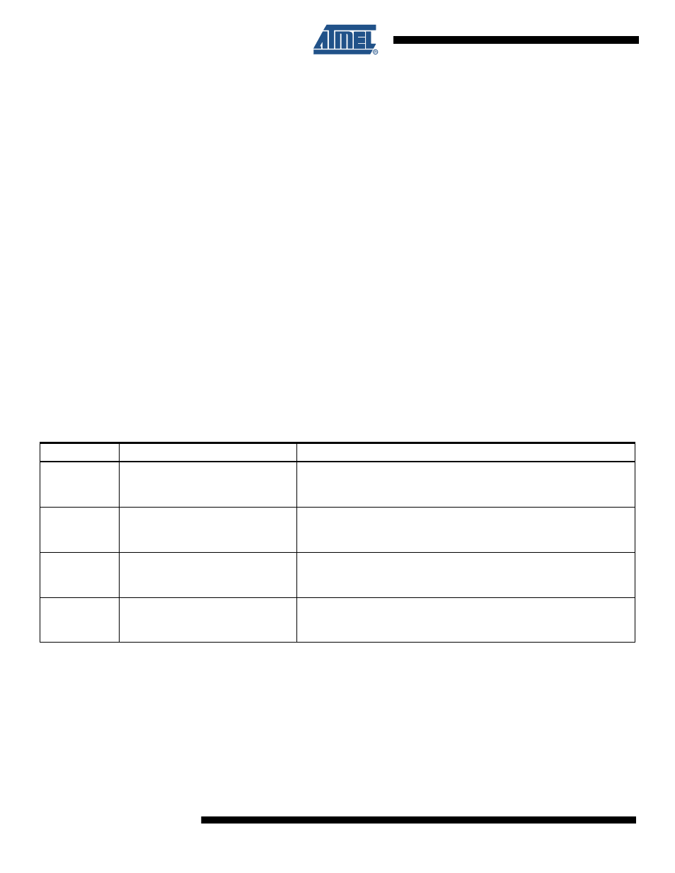
Table 1-2.
Analog Pin Behavior - DC values
Pin
Values and Conditions
Comments
RFP/RFN
V
DC
= 0.9V (BUSY_TX)
V
DC
= 20 mV (receive states)
V
DC
= 0 mV (otherwise)
DC level at pins RFP/RFN for various transceiver states
AC coupling is required if an antenna with a DC path to ground is used.
Serial capacitance and capacitance of each pin to ground must be < 30 pF.
XTAL1/ XTAL2
V
DC
= 0.9V at both pins
C
PAR
= 3 pF
DC level at pins XTAL1/XTAL2 for various transceiver states
Parasitic capacitance (C
PAR
) of the pins must be considered as additional
load capacitance to the crystal.
DVDD
V
DC
= 1.8V (all states, except SLEEP)
V
DC
= 0 mV (otherwise)
DC level at pin DVDD for various transceiver states
Supply pins (voltage regulator output) for the digital 1.8V voltage domain,
recommended bypass capacitor 1 µF.
AVDD
V
DC
= 1.8V (all states, except P_ON,
SLEEP, RESET, and TRX_OFF)
V
DC
= 0 mV (otherwise)
DC level at pin AVDD for various transceiver states
Supply pin (voltage regulator output) for the analog 1.8V voltage domain,
recommended bypass capacitor 1 µF.