5 data transfer - fast sram access, Section 11.1.5 “data transfer - fast sram, Section 11.1.5 – Rainbow Electronics AT86RF231 User Manual
Page 132
132
8111A–AVR–05/08
AT86RF231
Note that IEEE 802.15.4-2006 standard MIC algorithm requires CBC mode encryption only, as it
implements a one-way hash function.
11.1.5
Data Transfer - Fast SRAM Access
The ECB and CBC modules including the AES core are clocked with 16 MHz. One AES opera-
tion takes 24 µs to execute, refer to parameter 12.4.15 in
Section 12.4 “Digital Interface Timing
. That means that the processing of the data is usually faster than
the transfer of the data via the SPI interface.
To reduce the overall processing time the AT86RF231 provides a Fast SRAM access for the
address space 0x82 to 0x94.
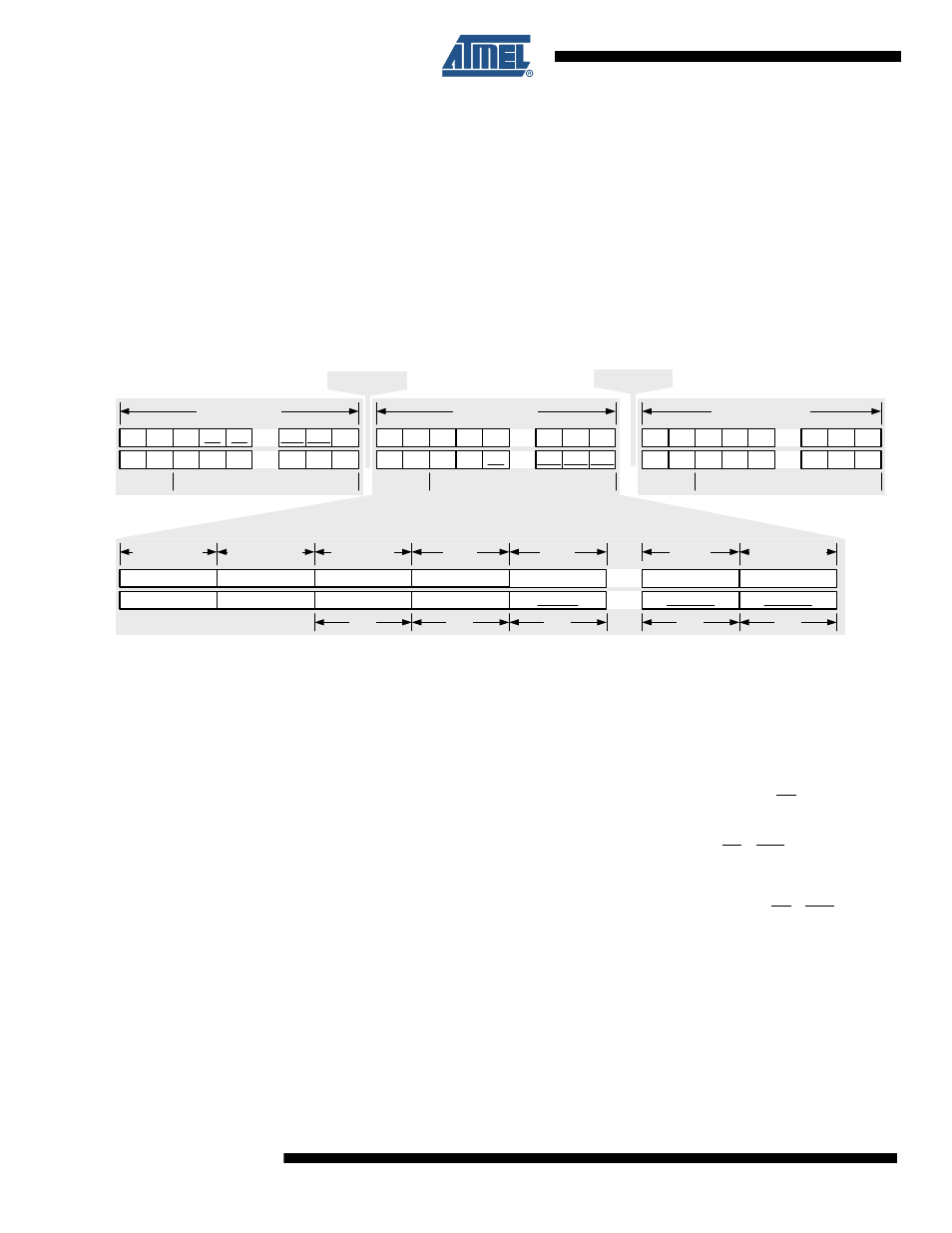
Figure 11-5. Packet Structure - Fast SRAM Access Mode
Note:
Byte 19 is the mirrored version of register AES_CON on SRAM address 0x94, see register
description AES_CON_MIRROR for details.
In contrast to a standard SRAM access, refer to
Section 6.2.3 “SRAM Access Mode” on page
, the Fast SRAM access allows writing and reading of data simultaneously during one SPI
access for consecutive AES operations (AES run).
For each byte P0 transferred to pin 22 (MOSI) for example in "AES access #1", see
(lower part), the previous content of the respective AES register C0 is clocked out
at pin 20 (MISO) with an offset of one byte.
In the example shown in
the initial plaintext P0 - P15 is written to the
SRAM within "AES access #0". The last command on address 0x94 (AES_CON_MIRROR)
starts the AES operation ("AES run #0"). In the next "AES access #1" new plaintext data P0 -
P15 is written to the SRAM for the second AES run, in parallel the ciphertext C0 - C15 from the
first AES run is clocked out at pin MISO. To read the ciphertext from the last "AES run #(n)" one
dummy "AES access #(n+1)" is needed.
Note that the SRAM write access always overwrites the previous processing result.
The Fast SRAM access automatically applies to all write operations to SRAM addresses 0x82 to
0x94.
SRAM write
MOSI
PHY_STATUS
MISO
byte 0 (cmd)
address 0x83
XX
XX
byte 1 (addr.)
byte 2 (cfg)
P0[7:0]
XX
byte 3
byte 4
byte 18
(1)
byte 19 (start)
0x83
0x85
0x84
0x93
0x94
Address
MOSI
MISO
AES access #0
Address
P0
P15
...
cmd add cfg
start
xx
xx
...
stat xx
xx
xx
0x83
0x94
...
AES access #1
P0
P15
...
cmd add cfg
start
xx
C14
...
stat xx
xx
C15
0x83
0x94
...
AES access #n+1
xx
xx
...
cmd add cfg
start
xx
C14
...
stat xx
xx
C15
0x83
0x94
...
P1
P14
xx
xx
P1
P14
C0
C13
xx
xx
C0
C13
...
...
C0[7:0]
P1[7:0]
C14[7:0]
C15[7:0]
P15[7:0]
AES run #0
AES run #n
..
.