3 external reference frequency setup, 4 master clock signal output (clkm), Section 9.6.4 – Rainbow Electronics AT86RF231 User Manual
Page 117: R details see
117
8111A–AVR–05/08
AT86RF231
Additional internal trimming capacitors C
TRIM
are available. Any value in the range from 0 pF to
4.5 pF with a 0.3 pF resolution is selectable using XTAL_TRIM of register 0x12 (XOSC_CTRL).
To calculate the total load capacitance, the following formula can be used
C
L
= 0.5 * (CX + C
TRIM
+ C
PAR
).
The trimming capacitors provide the possibility of reducing frequency deviations caused by pro-
duction process variations or by external components tolerances. Note that the oscillation
frequency can only be reduced by increasing the trimming capacitance. The frequency deviation
caused by one step of C
TRIM
decreases with increasing crystal load capacitor values.
An amplitude control circuit is included to ensure stable operation under different operating con-
ditions and for different crystal types. Enabling the crystal oscillator in P_ON state and after
leaving SLEEP state causes a slightly higher current during the amplitude build-up phase to
guarantee a short start-up time. At stable operation, the current is reduced to the amount neces-
sary for a robust operation. This also keeps the drive level of the crystal low.
Generally, crystals with a higher load capacitance are less sensitive to parasitic pulling effects
caused by external component variations or by variations of board and circuit parasitics. On the
other hand, a larger crystal load capacitance results in a longer start-up time and a higher steady
state current consumption.
9.6.3
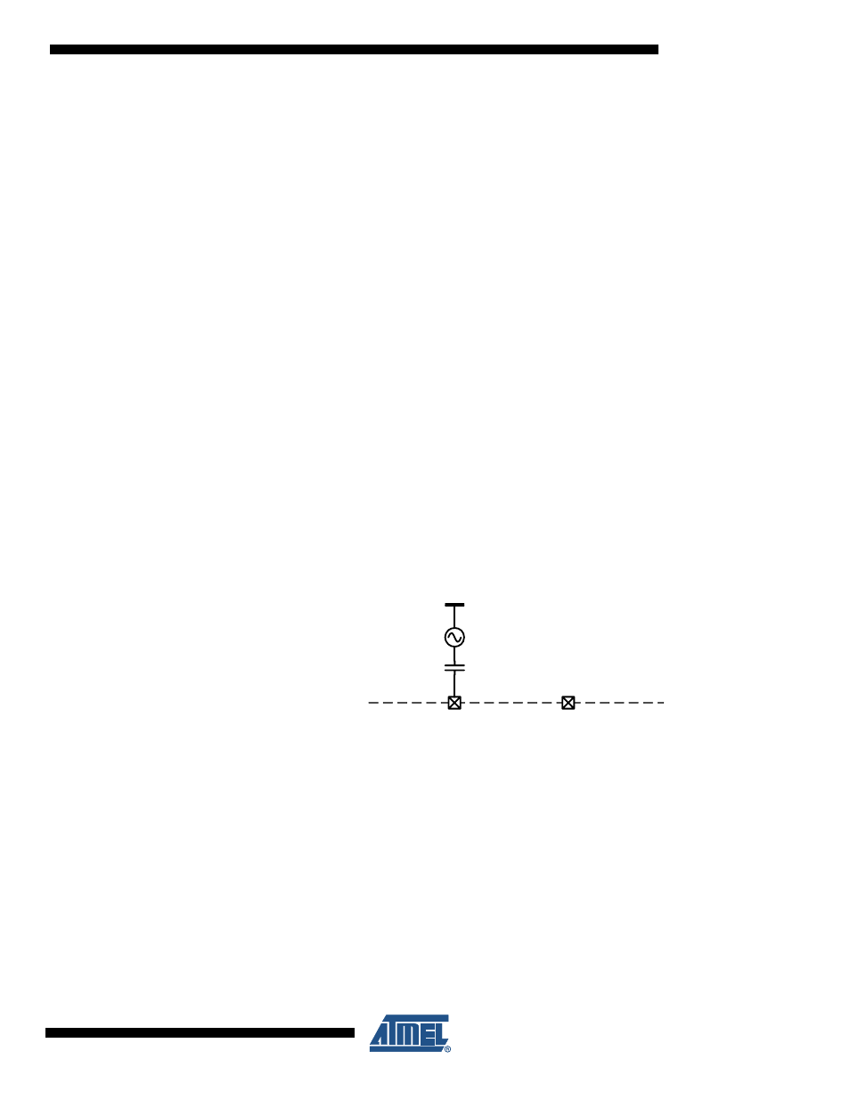
External Reference Frequency Setup
When using an external reference frequency, the signal must be connected to pin 26 (XTAL1) as
indicated in
and the register bits XTAL_MODE (register 0x12,
XOSC_CTRL) need to be set to the external oscillator mode. The oscillation peak-to-peak ampli-
tude shall be 400 mV, but not larger than 500 mV.
Figure 9-8.
Setup for Using an External Frequency Reference
9.6.4
Master Clock Signal Output (CLKM)
The generated reference clock signal can be fed to a microcontroller using pin 17 (CLKM). The
internal 16 MHz raw clock can be divided by an internal prescaler. Thus, clock frequencies of 16
MHz, 8 MHz, 4 MHz, 2 MHz, 1 MHz, 250 kHz, or 62.5 kHz can be supplied by pin CLKM.
The CLKM frequency and pin driver strength is configurable using register 0x03 (TRX_CTRL_0).
There are two possibilities to change the CLKM frequency. If CLKM_SHA_SEL = 0, changing
the register bits CLKM_CTRL (register 0x03, TRX_CTRL_0) immediately affects the CLKM
clock rate. Otherwise (CLKM_SHA_SEL = 1) the new clock rate is supplied when leaving the
SLEEP state the next time.
To reduce power consumption and spurious emissions, it is recommended to turn off the CLKM
clock when not in use or to reduce its driver strength to a minimum, refer to
XTAL2
XTAL1
AT86RF231
PCB
16 MHz