2 analog and rf pins, 1 supply and ground pins, 2 rf pins – Rainbow Electronics AT86RF231 User Manual
Page 5

5
8111A–AVR–05/08
AT86RF231
1.2
Analog and RF Pins
1.2.1
Supply and Ground Pins
EVDD, DEVDD
EVDD and DEVDD are analog and digital supply voltage pins of the AT86RF231 radio
transceiver.
AVDD, DVDD
AVDD and DVDD are outputs of the internal 1.8V voltage regulators. The voltage regulators are
controlled independently by the radio transceivers state machine and are activated dependent
on the current radio transceiver state. The voltage regulators can be configured for external
supply.
For details, refer to
Section 9.4 “Voltage Regulators (AVREG, DVREG)” on page 110
.
AVSS, DVSS
AVSS and DVSS are analog and digital ground pins respectively. The analog and digital power
domains should be separated on the PCB.
1.2.2
RF Pins
RFN, RFP
A differential RF port (RFP/RFN) provides common-mode rejection to suppress the switching
noise of the internal digital signal processing blocks. At board-level, the differential RF layout
ensures high receiver sensitivity by rejecting any spurious emissions originated from other digital
ICs such as a microcontroller.
The RF port is designed for a 100
Ω differential load. A DC path between the RF pins is allowed.
A DC path to ground or supply voltage is not allowed. Therefore, when connecting an RF-load
providing a DC path to the power supply or ground, AC-coupling is required as indicated in
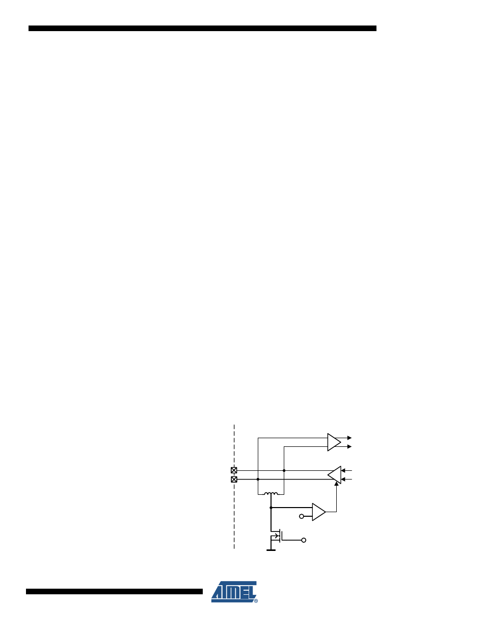
A simplified schematic of the RF front end is shown in
.
Figure 1-2.
Simplified RF Front-end Schematic
LNA
PA
RFP
RFN
RXTX
0.9V
TX
RX
CM
Feedback
M0
AT86RF231
PCB
